参数资料
| 型号: | XRT94L33IB-L |
| 厂商: | Exar Corporation |
| 文件页数: | 199/465页 |
| 文件大小: | 0K |
| 描述: | IC MAPPER DS3/E3/STS-1 504TBGA |
| 标准包装: | 24 |
| 应用: | 网络切换 |
| 接口: | 总线 |
| 电源电压: | 3.14 V ~ 3.47 V |
| 封装/外壳: | 504-LBGA |
| 供应商设备封装: | 504-TBGA(35x35) |
| 包装: | 托盘 |
| 安装类型: | 表面贴装 |
第1页第2页第3页第4页第5页第6页第7页第8页第9页第10页第11页第12页第13页第14页第15页第16页第17页第18页第19页第20页第21页第22页第23页第24页第25页第26页第27页第28页第29页第30页第31页第32页第33页第34页第35页第36页第37页第38页第39页第40页第41页第42页第43页第44页第45页第46页第47页第48页第49页第50页第51页第52页第53页第54页第55页第56页第57页第58页第59页第60页第61页第62页第63页第64页第65页第66页第67页第68页第69页第70页第71页第72页第73页第74页第75页第76页第77页第78页第79页第80页第81页第82页第83页第84页第85页第86页第87页第88页第89页第90页第91页第92页第93页第94页第95页第96页第97页第98页第99页第100页第101页第102页第103页第104页第105页第106页第107页第108页第109页第110页第111页第112页第113页第114页第115页第116页第117页第118页第119页第120页第121页第122页第123页第124页第125页第126页第127页第128页第129页第130页第131页第132页第133页第134页第135页第136页第137页第138页第139页第140页第141页第142页第143页第144页第145页第146页第147页第148页第149页第150页第151页第152页第153页第154页第155页第156页第157页第158页第159页第160页第161页第162页第163页第164页第165页第166页第167页第168页第169页第170页第171页第172页第173页第174页第175页第176页第177页第178页第179页第180页第181页第182页第183页第184页第185页第186页第187页第188页第189页第190页第191页第192页第193页第194页第195页第196页第197页第198页当前第199页第200页第201页第202页第203页第204页第205页第206页第207页第208页第209页第210页第211页第212页第213页第214页第215页第216页第217页第218页第219页第220页第221页第222页第223页第224页第225页第226页第227页第228页第229页第230页第231页第232页第233页第234页第235页第236页第237页第238页第239页第240页第241页第242页第243页第244页第245页第246页第247页第248页第249页第250页第251页第252页第253页第254页第255页第256页第257页第258页第259页第260页第261页第262页第263页第264页第265页第266页第267页第268页第269页第270页第271页第272页第273页第274页第275页第276页第277页第278页第279页第280页第281页第282页第283页第284页第285页第286页第287页第288页第289页第290页第291页第292页第293页第294页第295页第296页第297页第298页第299页第300页第301页第302页第303页第304页第305页第306页第307页第308页第309页第310页第311页第312页第313页第314页第315页第316页第317页第318页第319页第320页第321页第322页第323页第324页第325页第326页第327页第328页第329页第330页第331页第332页第333页第334页第335页第336页第337页第338页第339页第340页第341页第342页第343页第344页第345页第346页第347页第348页第349页第350页第351页第352页第353页第354页第355页第356页第357页第358页第359页第360页第361页第362页第363页第364页第365页第366页第367页第368页第369页第370页第371页第372页第373页第374页第375页第376页第377页第378页第379页第380页第381页第382页第383页第384页第385页第386页第387页第388页第389页第390页第391页第392页第393页第394页第395页第396页第397页第398页第399页第400页第401页第402页第403页第404页第405页第406页第407页第408页第409页第410页第411页第412页第413页第414页第415页第416页第417页第418页第419页第420页第421页第422页第423页第424页第425页第426页第427页第428页第429页第430页第431页第432页第433页第434页第435页第436页第437页第438页第439页第440页第441页第442页第443页第444页第445页第446页第447页第448页第449页第450页第451页第452页第453页第454页第455页第456页第457页第458页第459页第460页第461页第462页第463页第464页第465页
XRT94L33
xr
Rev.1.2.0.
3-CHANNEL DS3/E3/STS-1 TO STS-3/STM-1 MAPPER IC DATA SHEET
278
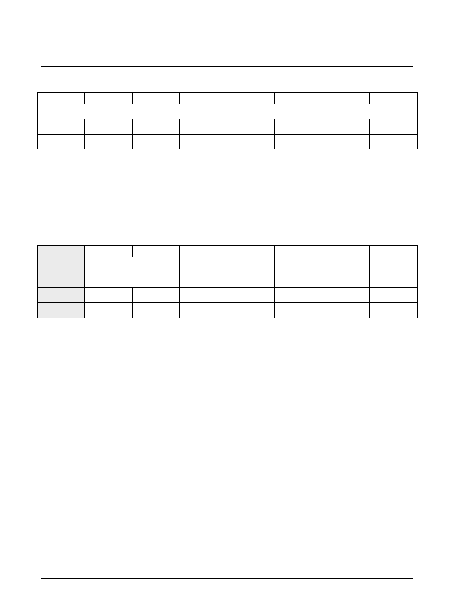
Transmit SONET Path – Transmit F2 Byte Value Register (Address = 0xN9A3)
BIT 7
BIT 6
BIT 5
BIT 4
BIT 3
BIT 2
BIT 1
BIT 0
Transmit_F2_Byte_Value[7:0]
R/W
0
2.2.8.3.6.2
Setting and Controlling the Outbound F2 Byte via the “TxPOH_n Input Port”
The Transmit SONET POH Processor block permits the user to specify the contents of the F2 byte, within the
“outbound” STS-1 SPE, via data applied to the “TxPOH_n” input pin.
The user can configure the Transmit SONET POH Processor block to accomplish this by performing the
following steps.
STEP 1 – Write the value “1” into Bit 7 (F2 Byte Insertion Type) within the “Transmit SONET Path –
SONET Control Register – Byte 0”, as depicted below.
Transmit SONET Path – SONET Control Register – Byte 0 (Address = 0xN983)
BIT 7
BIT 6
BIT 5
BIT 4
BIT 3
BIT 2
BIT 1
BIT 0
F2 Insertion
Type
REI-P Insertion Type[1:0]
RDI-P Insertion Type[1:0]
C2 Byte
Insertion
Type
Unused
Transmit
AIS-P
Enable
R/W
R/O
R/W
1
0
This step configures the Transmit SONET POH Processor block to use the “TxPOH_n” input port as the
source for the F2 byte, within each “outbound” STS-1 SPE.
In this mode, the Transmit SONET POH
Processor block will accept the value, corresponding to the F2 byte (via the “TxPOH_n” input port) and it will
write this data into the F2 byte position, within the “outbound” STS-1 SPE.
STEP 2 – Begin providing the values of the “outbound” F2 byte to the “TxPOH_n” input port.
The procedure for applying the F2 byte to the “TxPOH_n” input port is presented below.
Using the “TxPOH” Input Port to insert the F2 byte value into the outbound STS-1 SPE data-stream
If the user intends to externally insert the F2 byte into the outbound STS-1 SPE, via the “TxPOH_n” input port,
then they must design some external circuitry (which can be realized in an ASIC, FPGA or CPLD solution) to
do to the following.
Continuously sample the “TxPOHEnable_n” and the “TxPOHFrame_n” output pins upon the rising edge of
the “TxPOHClk_n” output clock signal.
A simple illustration of this “external circuit” being interfaced to the “TxPOH Input Port” is presented below in
Figure 52: A Simple Illustration of the “External Circuit” being interfaced to the “TxPOH Input Port”
相关PDF资料 |
PDF描述 |
|---|---|
| XRT94L43IB-F | IC MAPPER SONET/SDH OC12 516BGA |
| XS1-G02B-FB144-I4 | IC MCU 32BIT 16KB OTP 144FBGA |
| XTR114U/2K5 | IC 4-20MA I-TRANSMITTER 14-SOIC |
| ZXHF5000JB24TC | IC SWITCH QUAD 2X1 24QFN |
| 3341-56 | IC PLL INTEGER-N 3GHZ 20QFN |
相关代理商/技术参数 |
参数描述 |
|---|---|
| XRT94L43 | 制造商:EXAR 制造商全称:EXAR 功能描述:SONET/SDH STS-12/STM-4 TO E3/DS3/STS-1 MAPPER/DEMAPPER |
| XRT94L43_06 | 制造商:EXAR 制造商全称:EXAR 功能描述:SONET/SDH OC-12 TO 12XDS3/E3 MAPPER |
| XRT94L43A | 制造商:EXAR 制造商全称:EXAR 功能描述:SONET/SDH OC-12 TO 12XDS3/E3 MAPPER |
| XRT94L43ES-L03 | 功能描述:界面开发工具 Eval System for XRT94L43 Series RoHS:否 制造商:Bourns 产品:Evaluation Boards 类型:RS-485 工具用于评估:ADM3485E 接口类型:RS-485 工作电源电压:3.3 V |
| XRT94L43ES-LC03 | 功能描述:时钟合成器/抖动清除器 OC12-12XDS3MAPPER SCORPION 4x T73LC03A RoHS:否 制造商:Skyworks Solutions, Inc. 输出端数量: 输出电平: 最大输出频率: 输入电平: 最大输入频率:6.1 GHz 电源电压-最大:3.3 V 电源电压-最小:2.7 V 封装 / 箱体:TSSOP-28 封装:Reel |
发布紧急采购,3分钟左右您将得到回复。