- 您现在的位置:买卖IC网 > PDF目录15042 > ZL2008ALAFT (Intersil)IC REG CTRLR BUCK PWM VM 36-QFN PDF资料下载
参数资料
| 型号: | ZL2008ALAFT |
| 厂商: | Intersil |
| 文件页数: | 24/42页 |
| 文件大小: | 0K |
| 描述: | IC REG CTRLR BUCK PWM VM 36-QFN |
| 标准包装: | 100 |
| PWM 型: | 电压模式 |
| 输出数: | 1 |
| 频率 - 最大: | 1.4MHz |
| 占空比: | 95% |
| 电源电压: | 3 V ~ 5.5 V |
| 降压: | 是 |
| 升压: | 无 |
| 回扫: | 无 |
| 反相: | 无 |
| 倍增器: | 无 |
| 除法器: | 无 |
| Cuk: | 无 |
| 隔离: | 无 |
| 工作温度: | -40°C ~ 85°C |
| 封装/外壳: | 36-VFQFN 裸露焊盘 |
| 包装: | 带卷 (TR) |
第1页第2页第3页第4页第5页第6页第7页第8页第9页第10页第11页第12页第13页第14页第15页第16页第17页第18页第19页第20页第21页第22页第23页当前第24页第25页第26页第27页第28页第29页第30页第31页第32页第33页第34页第35页第36页第37页第38页第39页第40页第41页第42页
�� �
�
�ZL2008�
�Non-linear� Response� (NLR)� Settings�
�The� ZL2008� incorporates� a� non-linear� response� (NLR)� loop� that�
�decreases� the� response� time� and� the� output� voltage� deviation� in�
�the� event� of� a� sudden� output� load� current� step.� The� NLR� loop�
�incorporates� a� secondary� error� signal� processing� path� that�
�bypasses� the� primary� error� loop� when� the� output� begins� to�
�transition� outside� of� the� standard� regulation� limits.� This� scheme�
�results� in� a� higher� equivalent� loop� bandwidth� than� what� is�
�possible� using� a� traditional� linear� loop.�
�When� a� load� current� step� function� imposed� on� the� output� causes�
�the� output� voltage� to� drop� below� the� lower� regulation� limit,� the�
�NLR� circuitry� will� force� a� positive� correction� signal� that� will� turn�
�on� the� upper� MOSFET� and� quickly� force� the� output� to� increase.�
�Conversely,� a� negative� load� step� (i.e.� removing� a� large� load�
�current)� will� cause� the� NLR� circuitry� to� force� a� negative� correction�
�signal� that� will� turn� on� the� lower� MOSFET� and� quickly� force� the�
�output� to� decrease.�
�Adaptive� Diode� Emulation�
�Most� power� converters� use� synchronous� rectification� to� optimize�
�efficiency� over� a� wide� range� of� input� and� output� conditions.�
�However,� at� light� loads� the� synchronous� MOSFET� will� typically�
�sink� current� and� introduce� additional� energy� losses� associated�
�with� higher� peak� inductor� currents,� resulting� in� reduced�
�efficiency.� Adaptive� diode� emulation� mode� turns� off� the� low-side�
�FET� gate� drive� at� low� load� currents� to� prevent� the� inductor� current�
�from� going� negative,� reducing� the� energy� losses� and� increasing�
�overall� efficiency.� Diode� emulation� is� available� to� single-phase�
�devices� only.�
�Note:� the� overall� bandwidth� of� the� device� may� be� reduced� when�
�in� diode� emulation� mode.� It� is� recommended� that� diode�
�emulation� is� disabled� prior� to� applying� significant� load� steps.�
�Adaptive� Frequency� Control�
�Since� switching� losses� contribute� to� the� efficiency� of� the� power�
�NLR� can� be� configured� using� resistor� pin-straps� as� follows:�
�CFG0� disables� NLR� or� enables� NLR� inner� thresholds� to�
�2%� or� 3%� (see� Table� 30).�
�CFG1� sets� NLR� inner� thresholds� timeout� and� blanking�
�and� 4� or� 2� and� 8� (see� Table� 27).�
�1.5%,�
�to� 1�
�converter,� reducing� the� switching� frequency� will� reduce� the�
�switching� losses� and� increase� efficiency.� The� ZL2008� includes�
�Adaptive� Frequency� Control� mode,� which� effectively� reduces� the�
�observed� switching� frequency� as� the� load� decreases.�
�Adaptive� frequency� mode� is� enabled� by� setting� bit� 0� of�
�MISC_CONFIG� to� 1� and� is� only� available� while� the� device� is�
�Please� refer� to� Application� Note� AN2032� for� more� details�
�regarding� NLR� settings.�
�Efficiency� Optimized� Driver� Dead-time�
�Control�
�The� ZL2008� utilizes� a� closed� loop� algorithm� to� optimize� the�
�dead-time� applied� between� the� gate� drive� signals� for� the� top� and�
�bottom� FETs.� In� a� synchronous� buck� converter,� the� MOSFET� drive�
�circuitry� must� be� designed� such� that� the� top� and� bottom�
�MOSFETs� are� never� in� the� conducting� state� at� the� same� time.�
�Potentially� damaging� currents� flow� in� the� circuit� if� both� top� and�
�bottom� MOSFETs� are� simultaneously� on� for� periods� of� time�
�exceeding� a� few� nanoseconds.� Conversely,� long� periods� of� time� in�
�which� both� MOSFETs� are� off� reduce� overall� circuit� efficiency� by�
�allowing� current� to� flow� in� their� parasitic� body� diodes.�
�operating� within� Adaptive� Diode� Emulation� Mode.� As� the� load�
�current� is� decreased,� diode� emulation� mode� decreases� the� GL�
�on-time� to� prevent� negative� inductor� current� from� flowing.� As� the�
�load� is� decreased� further,� the� GH� pulse� width� will� begin� to�
�decrease� while� maintaining� the� programmed� frequency,� f� PROG�
�(set� by� the� FREQ_SWITCH� command).�
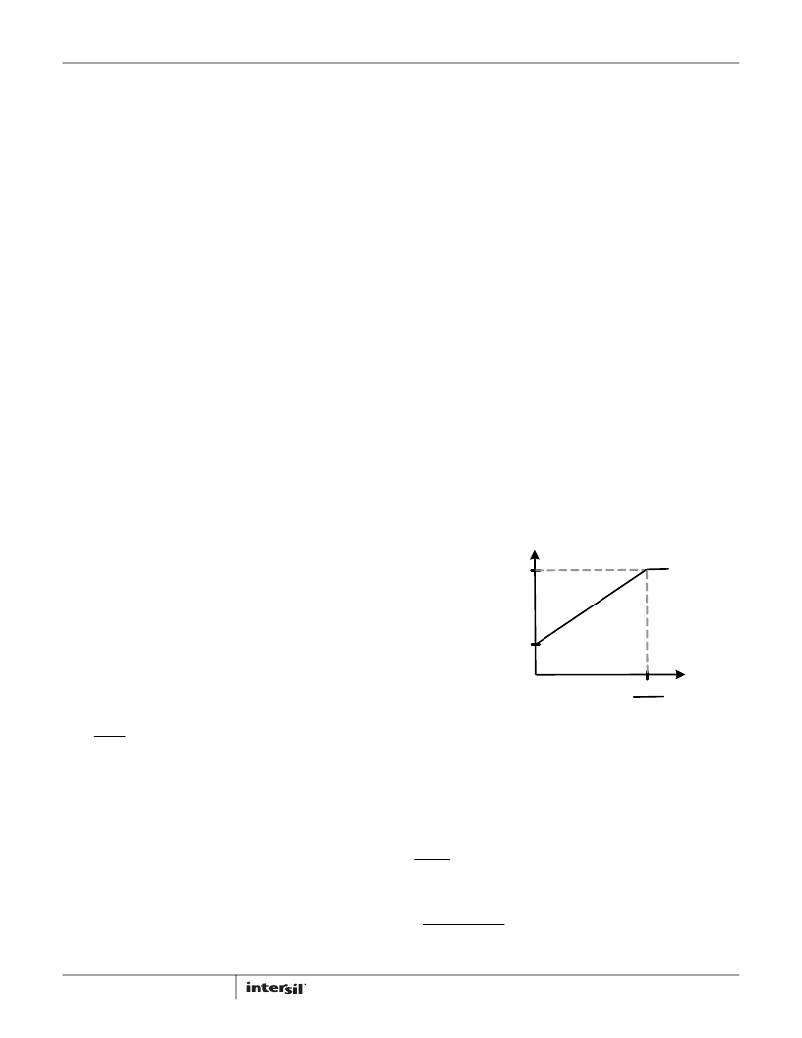
�f� SW� (D)�
�f� PROG�
�f� MIN�
�It� is� therefore� advantageous� to� minimize� this� dead-time� to�
�provide� optimum� circuit� efficiency.� In� the� first� order� model� of� a�
�buck� converter,� the� duty� cycle� is� determined� by� Equation� 32:�
�0�
�D� NOM�
�2�
�D�
�D� ≈�
�V� OUT�
�V� IN�
�(EQ.� 32)�
�Duty� Cycle�
�FIGURE� 18.� Adaptive� Frequency�
�However,� non-idealities� exist� that� cause� the� real� duty� cycle� to�
�extend� beyond� the� ideal.� Dead-time� is� one� of� those� non-idealities�
�that� can� be� manipulated� to� improve� efficiency.� The� ZL2008� has�
�an� internal� algorithm� that� constantly� adjusts� dead-time� non-�
�overlap� to� minimize� duty� cycle,� thus� maximizing� efficiency.� This�
�Once� the� GH� pulse� width� (D)� reaches� 50%� of� the� nominal� duty�
�cycle,� D� NOM� (determined� by� Vin� and� Vout),� the� switching�
�frequency� will� start� to� decrease� according� to� Equation� 33:�
�If�
�?� D� +� f� MIN�
�?� 2� (� f� SW� ?� f� MIN� )� ?�
�circuit� will� null� out� dead-time� differences� due� to� component�
�variation,� temperature,� and� loading� effects.�
�This� algorithm� is� independent� of� application� circuit� parameters�
�such� as� MOSFET� type,� gate� driver� delays,� rise� and� fall� times� and�
�circuit� layout.� In� addition,� it� does� not� require� drive� or� MOSFET�
�voltage� or� current� waveform� measurements.�
�24�
�D� NOM�
�2�
�then,�
�?�
�?� D� NOM� ?�
�(EQ.� 33)�
�FN6859.4�
�April� 29,� 2011�
�相关PDF资料 |
PDF描述 |
|---|---|
| VI-JWX-EW-F4 | CONVERTER MOD DC/DC 5.2V 100W |
| VI-J6X-EW-F2 | CONVERTER MOD DC/DC 5.2V 100W |
| VI-JWX-EW-F3 | CONVERTER MOD DC/DC 5.2V 100W |
| VI-JWX-EW-F1 | CONVERTER MOD DC/DC 5.2V 100W |
| VI-J6W-EW-F2 | CONVERTER MOD DC/DC 5.5V 100W |
相关代理商/技术参数 |
参数描述 |
|---|---|
| ZL2008ALAFT1 | 功能描述:IC REG CTRLR BUCK PWM VM 36-QFN RoHS:是 类别:集成电路 (IC) >> PMIC - 稳压器 - DC DC 切换控制器 系列:- 标准包装:2,500 系列:- PWM 型:电流模式 输出数:1 频率 - 最大:500kHz 占空比:100% 电源电压:8.2 V ~ 30 V 降压:无 升压:无 回扫:是 反相:无 倍增器:无 除法器:无 Cuk:无 隔离:是 工作温度:0°C ~ 70°C 封装/外壳:8-DIP(0.300",7.62mm) 包装:管件 产品目录页面:1316 (CN2011-ZH PDF) |
| ZL2008ALBFT | 功能描述:IC REG CTRLR BUCK PWM VM 36-QFN RoHS:是 类别:集成电路 (IC) >> PMIC - 稳压器 - DC DC 切换控制器 系列:- 产品培训模块:Lead (SnPb) Finish for COTS Obsolescence Mitigation Program 标准包装:2,500 系列:- PWM 型:电流模式 输出数:1 频率 - 最大:275kHz 占空比:50% 电源电压:18 V ~ 110 V 降压:无 升压:无 回扫:无 反相:无 倍增器:无 除法器:无 Cuk:无 隔离:是 工作温度:-40°C ~ 85°C 封装/外壳:8-SOIC(0.154",3.90mm 宽) 包装:带卷 (TR) |
| ZL2008ALBFT1 | 功能描述:IC REG CTRLR BUCK PWM VM 36-QFN RoHS:是 类别:集成电路 (IC) >> PMIC - 稳压器 - DC DC 切换控制器 系列:- 产品培训模块:Lead (SnPb) Finish for COTS Obsolescence Mitigation Program 标准包装:2,500 系列:- PWM 型:电流模式 输出数:1 频率 - 最大:275kHz 占空比:50% 电源电压:18 V ~ 110 V 降压:无 升压:无 回扫:无 反相:无 倍增器:无 除法器:无 Cuk:无 隔离:是 工作温度:-40°C ~ 85°C 封装/外壳:8-SOIC(0.154",3.90mm 宽) 包装:带卷 (TR) |
| ZL2008EVAL1Z | 功能描述:EVALUATION BOARD FOR ZL2008 RoHS:是 类别:编程器,开发系统 >> 评估板 - DC/DC 与 AC/DC(离线)SMPS 系列:- 产品培训模块:Obsolescence Mitigation Program 标准包装:1 系列:True Shutdown™ 主要目的:DC/DC,步升 输出及类型:1,非隔离 功率 - 输出:- 输出电压:- 电流 - 输出:1A 输入电压:2.5 V ~ 5.5 V 稳压器拓扑结构:升压 频率 - 开关:3MHz 板类型:完全填充 已供物品:板 已用 IC / 零件:MAX8969 |
| ZL20200 | 制造商:ZARLINK 制造商全称:Zarlink Semiconductor Inc 功能描述:Dual Band IS136/AMPS Transceiver |
发布紧急采购,3分钟左右您将得到回复。