- 您现在的位置:买卖IC网 > PDF目录15042 > ZL2008ALAFT (Intersil)IC REG CTRLR BUCK PWM VM 36-QFN PDF资料下载
参数资料
| 型号: | ZL2008ALAFT |
| 厂商: | Intersil |
| 文件页数: | 31/42页 |
| 文件大小: | 0K |
| 描述: | IC REG CTRLR BUCK PWM VM 36-QFN |
| 标准包装: | 100 |
| PWM 型: | 电压模式 |
| 输出数: | 1 |
| 频率 - 最大: | 1.4MHz |
| 占空比: | 95% |
| 电源电压: | 3 V ~ 5.5 V |
| 降压: | 是 |
| 升压: | 无 |
| 回扫: | 无 |
| 反相: | 无 |
| 倍增器: | 无 |
| 除法器: | 无 |
| Cuk: | 无 |
| 隔离: | 无 |
| 工作温度: | -40°C ~ 85°C |
| 封装/外壳: | 36-VFQFN 裸露焊盘 |
| 包装: | 带卷 (TR) |
第1页第2页第3页第4页第5页第6页第7页第8页第9页第10页第11页第12页第13页第14页第15页第16页第17页第18页第19页第20页第21页第22页第23页第24页第25页第26页第27页第28页第29页第30页当前第31页第32页第33页第34页第35页第36页第37页第38页第39页第40页第41页第42页
�� �
�
�ZL2008�
�Output� Sequencing�
�A� group� of� Digital-DC� devices� may� be� configured� to� power� up� in� a�
�predetermined� sequence.� This� feature� is� especially� useful� when�
�powering� advanced� processors,� FPGAs,� and� ASICs� that� require�
�one� supply� to� reach� its� operating� voltage� prior� to� another� supply�
�reaching� its� operating� voltage� in� order� to� avoid� latch-up� from�
�occurring.� Multi-device� sequencing� can� be� achieved� by�
�configuring� each� device� through� the� I� 2� C/SMBus� interface� or� by�
�using� Zilker� Labs� patented� autonomous� sequencing� mode.�
�Autonomous� sequencing� mode� configures� sequencing� by� using�
�events� transmitted� between� devices� over� the� DDC� bus.� This� mode�
�is� not� available� on� current� sharing� rails.�
�The� sequencing� order� is� determined� using� each� device’s� SMBus�
�address.� Using� autonomous� sequencing� mode� (configured� using�
�the� CFG1� pin),� the� devices� must� be� assigned� sequential� SMBus�
�addresses� with� no� missing� addresses� in� the� chain.� This� mode� will�
�also� constrain� each� device� to� have� a� phase� offset� according� to� its�
��Fault� Spreading�
�Digital� DC� devices� can� be� configured� to� broadcast� a� fault� event�
�over� the� DDC� bus� to� the� other� devices� in� the� group.� When� a� non-�
�destructive� fault� occurs� and� the� device� is� configured� to� shut� down�
�on� a� fault,� the� device� will� shut� down� and� broadcast� the� fault�
�event� over� the� DDC� bus.� The� other� devices� on� the� DDC� bus� will�
�shut� down� together� or� in� sequencing� order,� if� configured� to� do� so,�
�and� will� attempt� to� re-start� in� their� prescribed� order� if� configured�
�to� do� so.�
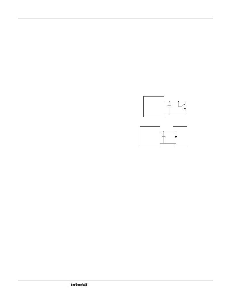
�Temperature� Monitoring� Using� the� XTEMP� Pin�
�The� ZL2008� supports� measurement� of� an� external� device�
�temperature� using� either� a� thermal� diode� integrated� in� a�
�processor,� FPGA� or� ASIC,� or� using� a� discrete� diode-connected�
�2N3904� NPN� transistor.� Figure� 21� illustrates� the� typical�
�connections� required.�
�XTEMP�
�The� sequencing� group� will� turn� on� in� order� starting� with� the�
�device� with� the� lowest� SMBus� address� and� will� continue� through�
�to� turn� on� each� device� in� the� address� chain� until� all� devices�
�connected� have� been� turned� on.� When� turning� off,� the� device�
�ZL�
�SGND�
�Discrete� NPN�
�100� pF�
�2N3904�
�with� the� highest� SMBus� address� will� turn� off� first� followed� in�
�reverse� order� by� the� other� devices� in� the� group.�
�Sequencing� is� configured� by� connecting� a� resistor� from� the� CFG1�
�pin� to� ground� as� described� in� Table� 27.� The� CFG1� pin� is� also� used�
�to� set� the� configuration� of� the� SYNC� pin� as� well� as� to� determine�
�ZL�
�XTEMP�
�SGND�
�100pF�
�μP�
�FPGA�
�DSP�
�ASIC�
�the� sequencing� method� and� order.� Please� refer� to� “Switching�
��parameters� of� the� SYNC� pin.�
�Multiple� device� sequencing� may� also� be� achieved� by� issuing�
�PMBus� commands� to� assign� the� preceding� device� in� the�
�sequencing� chain� as� well� as� the� device� that� will� follow� in� the�
�sequencing� chain.� This� method� places� fewer� restrictions� on�
�SMBus� address� (no� need� of� sequential� address)� and� also� allows�
�the� user� to� assign� any� phase� offset� to� any� device� irrespective� of�
�its� SMBus� device� address.�
�The� Enable� pins� of� all� devices� in� a� sequencing� group� must� be� tied�
�together� and� driven� high� to� initiate� a� sequenced� turn-on� of� the�
�group.� Enable� must� be� driven� low� to� initiate� a� sequenced� turnoff�
�of� the� group.�
�Refer� to� Application� Note� AN2033� for� details� on� sequencing� via�
�the� I� 2� C/SMBus� interface.�
�31�
�Embedded� Thermal� Diode�
�FIGURE� 21.� External� Temperature� Monitoring�
�Active� Current� Sharing�
�Paralleling� multiple� ZL2008� devices� can� be� used� to� increase� the�
�output� current� capability� of� a� single� power� rail.� By� connecting� the�
�DDC� pins� of� each� device� together� and� configuring� the� devices� as�
�a� current� sharing� rail,� the� units� will� share� the� current� equally�
�within� a� few� percent.�
�Figure� 22� illustrates� a� typical� connection� for� three� devices.�
�The� ZL2008� uses� a� low-bandwidth,� first-order� digital� current�
�sharing� technique� to� balance� the� unequal� device� output� loading�
�by� aligning� the� load� lines� of� member� devices� to� a� reference�
�device.�
�Droop� resistance� is� used� to� add� artificial� resistance� in� the� output�
�voltage� path� to� control� the� slope� of� the� load� line� curve,�
�calibrating� out� the� physical� parasitic� mismatches� due� to� power�
�train� components� and� PCB� layout.�
�FN6859.4�
�April� 29,� 2011�
�相关PDF资料 |
PDF描述 |
|---|---|
| VI-JWX-EW-F4 | CONVERTER MOD DC/DC 5.2V 100W |
| VI-J6X-EW-F2 | CONVERTER MOD DC/DC 5.2V 100W |
| VI-JWX-EW-F3 | CONVERTER MOD DC/DC 5.2V 100W |
| VI-JWX-EW-F1 | CONVERTER MOD DC/DC 5.2V 100W |
| VI-J6W-EW-F2 | CONVERTER MOD DC/DC 5.5V 100W |
相关代理商/技术参数 |
参数描述 |
|---|---|
| ZL2008ALAFT1 | 功能描述:IC REG CTRLR BUCK PWM VM 36-QFN RoHS:是 类别:集成电路 (IC) >> PMIC - 稳压器 - DC DC 切换控制器 系列:- 标准包装:2,500 系列:- PWM 型:电流模式 输出数:1 频率 - 最大:500kHz 占空比:100% 电源电压:8.2 V ~ 30 V 降压:无 升压:无 回扫:是 反相:无 倍增器:无 除法器:无 Cuk:无 隔离:是 工作温度:0°C ~ 70°C 封装/外壳:8-DIP(0.300",7.62mm) 包装:管件 产品目录页面:1316 (CN2011-ZH PDF) |
| ZL2008ALBFT | 功能描述:IC REG CTRLR BUCK PWM VM 36-QFN RoHS:是 类别:集成电路 (IC) >> PMIC - 稳压器 - DC DC 切换控制器 系列:- 产品培训模块:Lead (SnPb) Finish for COTS Obsolescence Mitigation Program 标准包装:2,500 系列:- PWM 型:电流模式 输出数:1 频率 - 最大:275kHz 占空比:50% 电源电压:18 V ~ 110 V 降压:无 升压:无 回扫:无 反相:无 倍增器:无 除法器:无 Cuk:无 隔离:是 工作温度:-40°C ~ 85°C 封装/外壳:8-SOIC(0.154",3.90mm 宽) 包装:带卷 (TR) |
| ZL2008ALBFT1 | 功能描述:IC REG CTRLR BUCK PWM VM 36-QFN RoHS:是 类别:集成电路 (IC) >> PMIC - 稳压器 - DC DC 切换控制器 系列:- 产品培训模块:Lead (SnPb) Finish for COTS Obsolescence Mitigation Program 标准包装:2,500 系列:- PWM 型:电流模式 输出数:1 频率 - 最大:275kHz 占空比:50% 电源电压:18 V ~ 110 V 降压:无 升压:无 回扫:无 反相:无 倍增器:无 除法器:无 Cuk:无 隔离:是 工作温度:-40°C ~ 85°C 封装/外壳:8-SOIC(0.154",3.90mm 宽) 包装:带卷 (TR) |
| ZL2008EVAL1Z | 功能描述:EVALUATION BOARD FOR ZL2008 RoHS:是 类别:编程器,开发系统 >> 评估板 - DC/DC 与 AC/DC(离线)SMPS 系列:- 产品培训模块:Obsolescence Mitigation Program 标准包装:1 系列:True Shutdown™ 主要目的:DC/DC,步升 输出及类型:1,非隔离 功率 - 输出:- 输出电压:- 电流 - 输出:1A 输入电压:2.5 V ~ 5.5 V 稳压器拓扑结构:升压 频率 - 开关:3MHz 板类型:完全填充 已供物品:板 已用 IC / 零件:MAX8969 |
| ZL20200 | 制造商:ZARLINK 制造商全称:Zarlink Semiconductor Inc 功能描述:Dual Band IS136/AMPS Transceiver |
发布紧急采购,3分钟左右您将得到回复。