- 您现在的位置:买卖IC网 > PDF目录370133 > 7549 (Renesas Technology Corp.) SINGLE-CHIP 8-BIT CMOS MICROCOMPUTER PDF资料下载
参数资料
| 型号: | 7549 |
| 厂商: | Renesas Technology Corp. |
| 英文描述: | SINGLE-CHIP 8-BIT CMOS MICROCOMPUTER |
| 中文描述: | 单芯片8位CMOS微机 |
| 文件页数: | 25/73页 |
| 文件大小: | 1272K |
| 代理商: | 7549 |
第1页第2页第3页第4页第5页第6页第7页第8页第9页第10页第11页第12页第13页第14页第15页第16页第17页第18页第19页第20页第21页第22页第23页第24页当前第25页第26页第27页第28页第29页第30页第31页第32页第33页第34页第35页第36页第37页第38页第39页第40页第41页第42页第43页第44页第45页第46页第47页第48页第49页第50页第51页第52页第53页第54页第55页第56页第57页第58页第59页第60页第61页第62页第63页第64页第65页第66页第67页第68页第69页第70页第71页第72页第73页
Rev.2.00
REJ03B0202-0200
Mar 05, 2007
Page 25 of 70
7549 Group
PRELIMINARY
Notice: This is not a final specification.
Some parametric limits are subject to change.
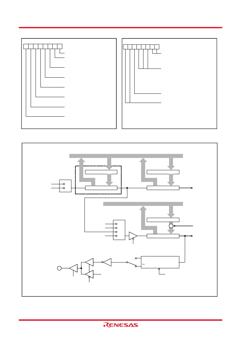
Fig 22. Structure of timer mode register
Fig 23. Structure of timer count source set register
Fig 24. Block diagram of timer 1 and timer 2
b7
b0
Timer mode register
(TM: address 002B
16
, initial value: 00
16
)
Not used (return “0” when read)
Timer 2 count stop bit
0: Count start
1: Count stop
P1
3
/T2
OUT
output valid bit
0: Pulse output invalid (I/O port)
1: Pulse output valid
T2
OUT
polarity selection bit
0: Start from “H” level
1: Start from “L” level
Timer 2 write control bit
0: Write to latch and timer simultaneously
1: Write to only latch
Timer A write control bit
0: Write to latch and timer simultaneously
1: Write to only latch
Timer A count stop bit
0: Count start
1: Count stop
Not used (return “0” when read)
b7
b0
Timer count source set register
(TCSS: address 002C
16
, initial value: 00
16
)
Timerb1 b0
φ
φ
SOURCE/16
0 0 :
Timerb4 b3 b2
φ
φ
φ
φ
φ
φ
SOURCE/16
0 0 (32kHz quartz crystal oscillation)
CIN
input clock
Prescaler 12 count source selection bit
SO input clock
CIN
0 :
Not used (return “0” when read)
Note 1:
φ
16
).
rSOURCE is the clock selected by bits 5 and 4 in the clock mode register (0037
Data bus
Timer 1
interrupt
request
φ
SOURCE/16
X
CIN
input clock
(32kHz quartz
crystal oscillation)
Data bus
Prescaler 12 latch (8)
Timer 1 latch (8)
Prescaler 12 (8)
Timer 1 (8)
φ
SOURCE/256
φ
SOURCE/16
Timer 2 count
stop bit
Timer 2 count
source selection bit
Prescaler 12 count
source selection bit
Timer 2
interrupt
request
Timer 2 latch (8)
Timer 2 (8)
Timer A underflow
Timer 2 write
control bit
Toggle flip-flop
T
Q
Q
P1
3
/T2
OUT
output valid bit
R
T2
OUT
polarity
selection bit
“1”
“0”
P1
3
/T2
OUT
output valid bit
Port P1
3
latch
Port P1
3
direction
register
P1
3
/T2
OUT
相关PDF资料 |
PDF描述 |
|---|---|
| 75HQ | SCHOTTKY RECTIFIER |
| 75HQ030 | SCHOTTKY RECTIFIER |
| 75HQ035 | SCHOTTKY RECTIFIER |
| 75HQ040 | SCHOTTKY RECTIFIER |
| 75HQ045 | SCHOTTKY RECTIFIER |
相关代理商/技术参数 |
参数描述 |
|---|---|
| 7549_0710 | 制造商:RENESAS 制造商全称:Renesas Technology Corp 功能描述:SINGLE-CHIP 8-BIT CMOS MICROCOMPUTER |
| 7549_09 | 制造商:RENESAS 制造商全称:Renesas Technology Corp 功能描述:SINGLE-CHIP 8-BIT CMOS MICROCOMPUTER |
| 7-5-4905 | 功能描述:3M 4905 VHB TAPE SPECIALTY TAPES 制造商:3m (tc) 系列:VHB?? 4905 零件状态:在售 厚度 - 粘合剂:- 厚度 - 底布,载体:- 标准包装:1 |
| 754905-1 | 功能描述:PIN ATT/ROLL AUTO IV 制造商:te connectivity amp connectors 系列:* 零件状态:有效 标准包装:1 |
| 7-5-4910 | 功能描述:3M 4910 VHB TAPE SPECIALTY TAPES 制造商:3m (tc) 系列:VHB?? 4910 零件状态:在售 底布,载体:丙烯酸泡棉 厚度 - 粘合剂:- 厚度 - 底布,载体:- 标准包装:1 |
发布紧急采购,3分钟左右您将得到回复。