- 您现在的位置:买卖IC网 > PDF目录370133 > 7549 (Renesas Technology Corp.) SINGLE-CHIP 8-BIT CMOS MICROCOMPUTER PDF资料下载
参数资料
| 型号: | 7549 |
| 厂商: | Renesas Technology Corp. |
| 英文描述: | SINGLE-CHIP 8-BIT CMOS MICROCOMPUTER |
| 中文描述: | 单芯片8位CMOS微机 |
| 文件页数: | 65/73页 |
| 文件大小: | 1272K |
| 代理商: | 7549 |
第1页第2页第3页第4页第5页第6页第7页第8页第9页第10页第11页第12页第13页第14页第15页第16页第17页第18页第19页第20页第21页第22页第23页第24页第25页第26页第27页第28页第29页第30页第31页第32页第33页第34页第35页第36页第37页第38页第39页第40页第41页第42页第43页第44页第45页第46页第47页第48页第49页第50页第51页第52页第53页第54页第55页第56页第57页第58页第59页第60页第61页第62页第63页第64页当前第65页第66页第67页第68页第69页第70页第71页第72页第73页
Rev.2.00
REJ03B0202-0200
Mar 05, 2007
Page 65 of 70
7549 Group
PRELIMINARY
Notice: This is not a final specification.
Some parametric limits are subject to change.
Power-on reset circuit characteristics
Power-on reset circuit characteristics
(V
CC
= 1.8 to 5.5 V, V
SS
= 0 V, Ta =
20 to 85
°
C, unless otherwise noted)
NOTE:
1. V
POR
is the start voltage level of Vcc for the built-in power-on reset circuit to operate normally.
Keep V
POR
to be lower than the Vcc voltage before rising of the Vcc power source to use the built-in power-on reset circuit.
Set the built-in low voltage detection circuit to be valid when the built-in power-on reset is used.
Low voltage detection circuit characteristics
Low voltage detection circuit characteristics
(V
CC
= 1.8 to 5.5 V, V
SS
= 0 V, Ta =
20 to 85
°
C, unless otherwise noted)
NOTE:
1. V
LVD
is the start voltage level of Vcc for the built-in low voltage detection circuit to operate normally.
If the Vcc power source becomes lower than V
LVD
, first set the Vcc voltage to be lower than V
POR
. Next, according to the electrical
characteristics of the power-on reset circuit, perform the rising of Vcc.
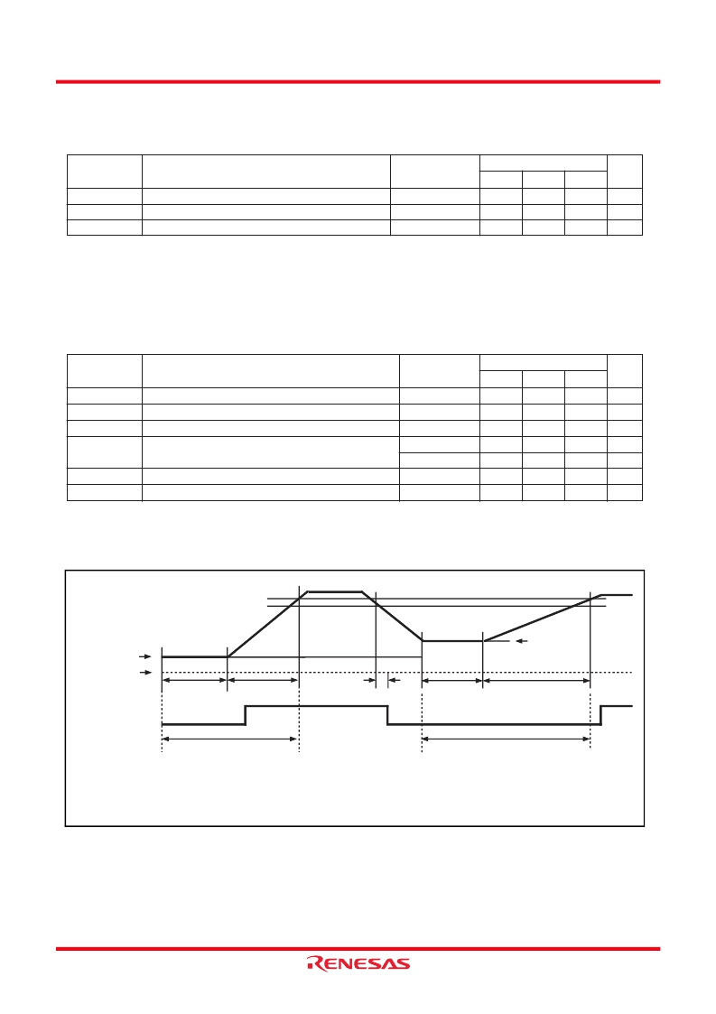
Fig 81. Electrical characteristics of power-on reset circuit and voltage drop detection circuit
V
POR
TW(V
POR
)
TW(V
POR
-V
DET
)
Valid start voltage of power-on reset circuit (Note)
V
POR
hold time
Rising time of valid power source of power-on reset circuit
Symbol
Parameter
Limits
Unit
Min.
Typ.
V
s
ms
Max.
0
10
20
TW(V
POR
) > 10s
Test conditions
V
LVD
TW(V
LVD
)
TW(V
LVD
-V
DET
)
V
DET-
V(V
DET+-
V
DET-
)
T
DET
Valid start voltage of low voltage detection circuit (Note)
V
LVD
hold time
Rising time of valid power source of low voltage detection circuit
Detection voltage of low voltage detection circuit
Detection voltage Hysteresis (when hysteresis is valid)
Detection time of low 5voltage detection circuit
Symbol
Parameter
Limits
Unit
Min.
1.0
1.85
1.80
Typ.
1.95
1.95
0.10
20
V
s
s
V
V
V
μ
s
Max.
10
10
2.05
2.10
TW(V
LVD
) > 10s
T
a
= 0
50 °C
T
a
=
20
85 °C
T
a
=
20
85 °C
Test conditions
Vcc power source
waveform
V
POR
0V
TW(V
POR
)T
T(V
PON
-V
DET
)
T
DET
TW(V
LVD
)T
T(V
LVD
-V
DET
)
Note
V
DET+
V
DET-
Internal reset signal
Power-on reset circuit
characteristics
Low voltage detection circuit
characteristics
V
POR
Note: If schmitt of the voltage drop detection circuit is set to be invalid, system is released from reset at the timing of rising to
power source voltage V
DET-
.
相关PDF资料 |
PDF描述 |
|---|---|
| 75HQ | SCHOTTKY RECTIFIER |
| 75HQ030 | SCHOTTKY RECTIFIER |
| 75HQ035 | SCHOTTKY RECTIFIER |
| 75HQ040 | SCHOTTKY RECTIFIER |
| 75HQ045 | SCHOTTKY RECTIFIER |
相关代理商/技术参数 |
参数描述 |
|---|---|
| 7549_0710 | 制造商:RENESAS 制造商全称:Renesas Technology Corp 功能描述:SINGLE-CHIP 8-BIT CMOS MICROCOMPUTER |
| 7549_09 | 制造商:RENESAS 制造商全称:Renesas Technology Corp 功能描述:SINGLE-CHIP 8-BIT CMOS MICROCOMPUTER |
| 7-5-4905 | 功能描述:3M 4905 VHB TAPE SPECIALTY TAPES 制造商:3m (tc) 系列:VHB?? 4905 零件状态:在售 厚度 - 粘合剂:- 厚度 - 底布,载体:- 标准包装:1 |
| 754905-1 | 功能描述:PIN ATT/ROLL AUTO IV 制造商:te connectivity amp connectors 系列:* 零件状态:有效 标准包装:1 |
| 7-5-4910 | 功能描述:3M 4910 VHB TAPE SPECIALTY TAPES 制造商:3m (tc) 系列:VHB?? 4910 零件状态:在售 底布,载体:丙烯酸泡棉 厚度 - 粘合剂:- 厚度 - 底布,载体:- 标准包装:1 |
发布紧急采购,3分钟左右您将得到回复。