- 您现在的位置:买卖IC网 > PDF目录370133 > 7549 (Renesas Technology Corp.) SINGLE-CHIP 8-BIT CMOS MICROCOMPUTER PDF资料下载
参数资料
| 型号: | 7549 |
| 厂商: | Renesas Technology Corp. |
| 英文描述: | SINGLE-CHIP 8-BIT CMOS MICROCOMPUTER |
| 中文描述: | 单芯片8位CMOS微机 |
| 文件页数: | 37/73页 |
| 文件大小: | 1272K |
| 代理商: | 7549 |
第1页第2页第3页第4页第5页第6页第7页第8页第9页第10页第11页第12页第13页第14页第15页第16页第17页第18页第19页第20页第21页第22页第23页第24页第25页第26页第27页第28页第29页第30页第31页第32页第33页第34页第35页第36页当前第37页第38页第39页第40页第41页第42页第43页第44页第45页第46页第47页第48页第49页第50页第51页第52页第53页第54页第55页第56页第57页第58页第59页第60页第61页第62页第63页第64页第65页第66页第67页第68页第69页第70页第71页第72页第73页
Rev.2.00
REJ03B0202-0200
Mar 05, 2007
Page 37 of 70
7549 Group
PRELIMINARY
Notice: This is not a final specification.
Some parametric limits are subject to change.
A/D Converter
The functional blocks of the A/D converter are described below.
[AD conversion register] AD
The A/D conversion register is a read-only register that stores the
result of A/D conversion. Do not read out this register during an
A/D conversion.
[AD control register] ADCON
The AD control register controls the A/D converter.
Bit 2 to 0 are analog input pin selection bits.
Bit 3 is the AD conversion clock selection bit. When “0” is set to
this bit, the A/D conversion clock is
φ
SOURCE/2 and the A/D
conversion time is 122 cycles of
φ
SOURCE. When “1” is set to
this bit, the A/D conversion clock is
φ
SOURCE and the A/D
conversion time is 61 cycles of
φ
SOURCE.
Bit 4 is the AD conversion completion bit. The value of this bit
remains at “0” during A/D conversion, and changes to “1” at
completion of A/D conversion.
A/D conversion is started by setting this bit to “0”.
[Comparison voltage generator]
The comparison voltage generator divides the voltage between
V
SS
and V
CC
by 1024, and outputs the divided voltages.
[Channel selector]
The channel selector selects one of ports P1
7
/AN
7
to P1
0
/AN
0,
and inputs the voltage to the comparator.
[Comparator and control circuit]
The comparator and control circuit compares an analog input
voltage with the comparison voltage and stores its result into the
AD conversion register. When A/D conversion is completed, the
control circuit sets the AD conversion completion bit and the A/
D interrupt request bit to “1”. Because the comparator is
constructed linked to a capacitor, set
φ
SOURCE in order that the
A/D conversion clock is 250 kHz or over during A/D conversion.
Notes on A/D converter
As for AD translation accuracy, on the following operating
conditions,
accuracy may become low.
(1) When V
CC
voltage is lower than [ 3.0 V ], the accuracy at
the low temperature may become extremely low compared
with that at room temperature. When the system would be
used at low temperature, the use at V
CC
= 3.0 V or more is
recommended.
(2) When X
CIN
or the low-speed on-chip oscillator is selected as
φ
SOURCE, the A/D converter cannot be used.
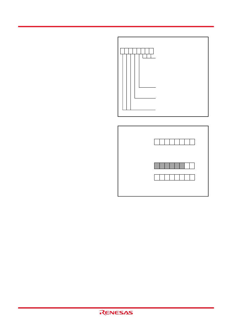
Fig 47. Structure of AD control register
Fig 48. Structure of AD conversion register
AD control register
(ADCON: address 0034
16
, initial value: 10
16
)
Analog input pin selection bits
000: P1
0
/AN
0
001: P1
1
/AN
1
010: P1
2
/AN
2
011: P1
3
/AN
3
100: P1
4
/AN
4
101: P1
5
/AN
5
110: P1
6
/AN
6
111: P1
7
/AN
7
AD conversion clock selection bit
0:
φ
SOURCE/2
1:
φ
SOURCE
AD conversion completion bit
0: Conversion in progress
1: Conversion completed
Not used (returns “0” when read)
b7
b0
Read 8-bit (Read only address 0035
16
)
(Address 0035
16
)
Read 10-bit (read in order address 0036
16
, 0035
16
)
b7
(Address 0036
16
)
(Address 0035
16
)
Note:
High-order 6-bit of address 0036
16
returns “0” when read.
b0
b9 b8
b7
b7
b0
b6 b5 b4 b3 b2 b1 b0
b9
b7
b0
b8 b7 b6 b5 b4 b3 b2
相关PDF资料 |
PDF描述 |
|---|---|
| 75HQ | SCHOTTKY RECTIFIER |
| 75HQ030 | SCHOTTKY RECTIFIER |
| 75HQ035 | SCHOTTKY RECTIFIER |
| 75HQ040 | SCHOTTKY RECTIFIER |
| 75HQ045 | SCHOTTKY RECTIFIER |
相关代理商/技术参数 |
参数描述 |
|---|---|
| 7549_0710 | 制造商:RENESAS 制造商全称:Renesas Technology Corp 功能描述:SINGLE-CHIP 8-BIT CMOS MICROCOMPUTER |
| 7549_09 | 制造商:RENESAS 制造商全称:Renesas Technology Corp 功能描述:SINGLE-CHIP 8-BIT CMOS MICROCOMPUTER |
| 7-5-4905 | 功能描述:3M 4905 VHB TAPE SPECIALTY TAPES 制造商:3m (tc) 系列:VHB?? 4905 零件状态:在售 厚度 - 粘合剂:- 厚度 - 底布,载体:- 标准包装:1 |
| 754905-1 | 功能描述:PIN ATT/ROLL AUTO IV 制造商:te connectivity amp connectors 系列:* 零件状态:有效 标准包装:1 |
| 7-5-4910 | 功能描述:3M 4910 VHB TAPE SPECIALTY TAPES 制造商:3m (tc) 系列:VHB?? 4910 零件状态:在售 底布,载体:丙烯酸泡棉 厚度 - 粘合剂:- 厚度 - 底布,载体:- 标准包装:1 |
发布紧急采购,3分钟左右您将得到回复。