- 您现在的位置:买卖IC网 > PDF目录370133 > 7549 (Renesas Technology Corp.) SINGLE-CHIP 8-BIT CMOS MICROCOMPUTER PDF资料下载
参数资料
| 型号: | 7549 |
| 厂商: | Renesas Technology Corp. |
| 英文描述: | SINGLE-CHIP 8-BIT CMOS MICROCOMPUTER |
| 中文描述: | 单芯片8位CMOS微机 |
| 文件页数: | 68/73页 |
| 文件大小: | 1272K |
| 代理商: | 7549 |
第1页第2页第3页第4页第5页第6页第7页第8页第9页第10页第11页第12页第13页第14页第15页第16页第17页第18页第19页第20页第21页第22页第23页第24页第25页第26页第27页第28页第29页第30页第31页第32页第33页第34页第35页第36页第37页第38页第39页第40页第41页第42页第43页第44页第45页第46页第47页第48页第49页第50页第51页第52页第53页第54页第55页第56页第57页第58页第59页第60页第61页第62页第63页第64页第65页第66页第67页当前第68页第69页第70页第71页第72页第73页
Rev.2.00
REJ03B0202-0200
Mar 05, 2007
Page 68 of 70
7549 Group
PRELIMINARY
Notice: This is not a final specification.
Some parametric limits are subject to change.
Switching Characteristics
Switching characteristics (1)
(V
CC
= 4.0 to 5.5 V, V
SS
= 0 V, Ta =
20 to 85
°
C, unless otherwise noted)
NOTE:
1. Pin X
OUT
is excluded.
Switching characteristics (2)
(V
CC
= 2.4 to 5.5 V, V
SS
= 0 V, Ta =
20 to 85
°
C, unless otherwise noted)
NOTE:
1. Pin X
OUT
is excluded.
Switching characteristics (3)
(V
CC
= 1.8 to 5.5 V, V
SS
= 0 V, Ta =
20 to 85
°
C, unless otherwise noted)
NOTE:
1. Pin X
OUT
is excluded.
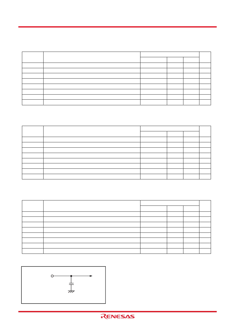
Fig 82. Switching characteristics measurement circuit diagram
t
WH
(S
CLK
)
t
WL
(S
CLK
)
t
d
(S
CLK
-T
X
D)
t
V
(S
CLK
-T
X
D)
t
r
(S
CLK
)
t
f
(S
CLK
)
t
r
(CMOS)
t
f
(CMOS)
Serial I/O clock output “H” pulse width
Serial I/O clock output “L” pulse width
Serial I/O output delay time
Serial I/O output valid time
Serial I/O clock output rising time
Serial I/O clock output falling time
CMOS output rising time (Note 1)
CMOS output falling time (Note 1)
Symbol
Parameter
Limits
Unit
Min.
t
C
(S
CLK
)/2
30
t
C
(S
CLK
)/2
30
30
Typ.
10
10
ns
ns
ns
ns
ns
ns
ns
ns
Max.
140
30
30
30
30
t
WH
(S
CLK
)
t
WL
(S
CLK
)
t
d
(S
CLK
-T
X
D)
t
V
(S
CLK
-T
X
D)
t
r
(S
CLK
)
t
f
(S
CLK
)
t
r
(CMOS)
t
f
(CMOS)
Serial I/O clock output “H” pulse width
Serial I/O clock output “L” pulse width
Serial I/O output delay time
Serial I/O output valid time
Serial I/O clock output rising time
Serial I/O clock output falling time
CMOS output rising time (Note 1)
CMOS output falling time (Note 1)
Symbol
Parameter
Limits
Unit
Min.
t
C
(S
CLK
)/2
50
t
C
(S
CLK
)/2
50
30
Typ.
20
20
ns
ns
ns
ns
ns
ns
ns
ns
Max.
350
50
50
50
50
t
WH
(S
CLK
)
t
WL
(S
CLK
)
t
d
(S
CLK
-T
X
D)
t
V
(S
CLK
-T
X
D)
t
r
(S
CLK
)
t
f
(S
CLK
)
t
r
(CMOS)
t
f
(CMOS)
Serial I/O clock output “H” pulse width
Serial I/O clock output “L” pulse width
Serial I/O output delay time
Serial I/O output valid time
Serial I/O clock output rising time
Serial I/O clock output falling time
CMOS output rising time (Note 1)
CMOS output falling time (Note 1)
Symbol
Parameter
Limits
Unit
Min.
t
C
(S
CLK
)/2
70
t
C
(S
CLK
)/2
70
30
Typ.
25
25
ns
ns
ns
ns
ns
ns
ns
ns
Max.
450
70
70
70
70
Measured
output pin
100pF
CMOS output
相关PDF资料 |
PDF描述 |
|---|---|
| 75HQ | SCHOTTKY RECTIFIER |
| 75HQ030 | SCHOTTKY RECTIFIER |
| 75HQ035 | SCHOTTKY RECTIFIER |
| 75HQ040 | SCHOTTKY RECTIFIER |
| 75HQ045 | SCHOTTKY RECTIFIER |
相关代理商/技术参数 |
参数描述 |
|---|---|
| 7549_0710 | 制造商:RENESAS 制造商全称:Renesas Technology Corp 功能描述:SINGLE-CHIP 8-BIT CMOS MICROCOMPUTER |
| 7549_09 | 制造商:RENESAS 制造商全称:Renesas Technology Corp 功能描述:SINGLE-CHIP 8-BIT CMOS MICROCOMPUTER |
| 7-5-4905 | 功能描述:3M 4905 VHB TAPE SPECIALTY TAPES 制造商:3m (tc) 系列:VHB?? 4905 零件状态:在售 厚度 - 粘合剂:- 厚度 - 底布,载体:- 标准包装:1 |
| 754905-1 | 功能描述:PIN ATT/ROLL AUTO IV 制造商:te connectivity amp connectors 系列:* 零件状态:有效 标准包装:1 |
| 7-5-4910 | 功能描述:3M 4910 VHB TAPE SPECIALTY TAPES 制造商:3m (tc) 系列:VHB?? 4910 零件状态:在售 底布,载体:丙烯酸泡棉 厚度 - 粘合剂:- 厚度 - 底布,载体:- 标准包装:1 |
发布紧急采购,3分钟左右您将得到回复。