参数资料
| 型号: | AD9852ASVZ |
| 厂商: | Analog Devices Inc |
| 文件页数: | 11/52页 |
| 文件大小: | 0K |
| 描述: | IC DDS SYNTHESIZER CMOS 80-TQFP |
| 产品培训模块: | Direct Digital Synthesis Tutorial Series (1 of 7): Introduction Direct Digital Synthesizer Tutorial Series (7 of 7): DDS in Action Direct Digital Synthesis Tutorial Series (3 of 7): Angle to Amplitude Converter Direct Digital Synthesis Tutorial Series (6 of 7): SINC Envelope Correction Direct Digital Synthesis Tutorial Series (4 of 7): Digital-to-Analog Converter Direct Digital Synthesis Tutorial Series (2 of 7): The Accumulator |
| 标准包装: | 1 |
| 分辨率(位): | 12 b |
| 主 fclk: | 300MHz |
| 调节字宽(位): | 48 b |
| 电源电压: | 3.14 V ~ 3.47 V |
| 工作温度: | -40°C ~ 85°C |
| 安装类型: | 表面贴装 |
| 封装/外壳: | 80-TQFP 裸露焊盘 |
| 供应商设备封装: | 80-TQFP-EP(12x12) |
| 包装: | 托盘 |
| 配用: | AD9852/PCBZ-ND - BOARD EVAL FOR AD9852 |
第1页第2页第3页第4页第5页第6页第7页第8页第9页第10页当前第11页第12页第13页第14页第15页第16页第17页第18页第19页第20页第21页第22页第23页第24页第25页第26页第27页第28页第29页第30页第31页第32页第33页第34页第35页第36页第37页第38页第39页第40页第41页第42页第43页第44页第45页第46页第47页第48页第49页第50页第51页第52页
AD9852
Rev. E | Page 19 of 52
Table 7. Function Availability vs. Mode of Operation
Function
Single-Tone Mode
FSK Mode
Ramped FSK Mode
Chirp Mode
BPSK Mode
Phase Adjust 1
●
Phase Adjust 2
●
Single-Pin FSK/BPSK or HOLD
●
Single-Pin Output Shaped Keying
●
Phase Offset or Modulation
●
Amplitude Control or Modulation
●
Inverse Sinc Filter
●
Frequency Tuning Word 1
●
Frequency Tuning Word 2
●
Automatic Frequency Sweep
●
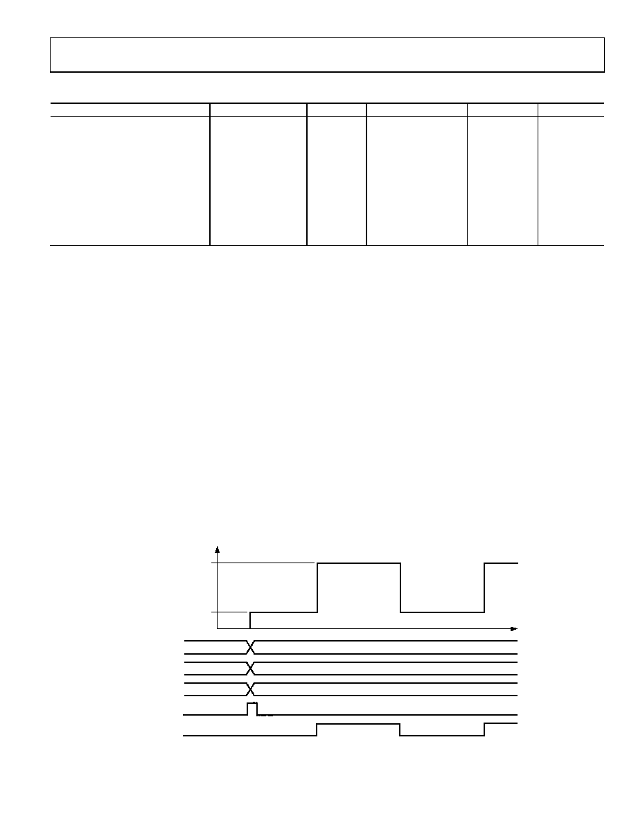
UNRAMPED FSK (MODE 001)
When this mode is selected, the output frequency of the DDS is
a function of the values loaded into Frequency Tuning Word
Register 1 and Frequency Tuning Word Register 2 and the logic
level of Pin 29 (FSK/BPSK/HOLD). A logic low on Pin 29
chooses F1 (Frequency Tuning Word 1, Parallel Address 4 hex
to Parallel Address 9 hex), and a logic high chooses F2
(Frequency Tuning Word 2, Parallel Register Address A hex to
Parallel Register Address F hex). Changes in frequency are
phase continuous and are internally coincident with the FSK
data pin (Pin 29); however, there is deterministic pipeline delay
between the FSK data signal and the DAC output (see Table 1).
The unramped FSK mode (see Figure 33) is representative
of traditional FSK, radio teletype (RTTY), or teletype (TTY)
transmission of digital data. FSK is a very reliable means of
digital communication; however, it makes inefficient use of
the bandwidth in the RF spectrum. Ramped FSK, shown in
Figure 34, is a method of conserving the bandwidth.
RAMPED FSK (MODE 010)
In this method of FSK, changes from F1 to F2 are not
instantaneous, but are accomplished in a frequency sweep or
ramped fashion. The ramped notation implies the sweep is
linear. Although linear sweeping, or frequency ramping, is
easily and automatically accomplished, it is only one of many
possibilities. Other frequency transition schemes can be
implemented by changing the ramp rate and ramp step size at
any time during operation.
Frequency ramping, whether linear or nonlinear, necessitates
that many intermediate frequencies between F1 and F2 are
output in addition to the primary F1 and F2 frequencies.
time characteristics of a linear ramped FSK signal.
In ramped FSK mode, the delta frequency word (DFW) is
required to be programmed as a positive twos complement
value. Another requirement is that the lowest frequency (F1) be
programmed in the Frequency Tuning Word 1 registers.
F1
F2
0
FREQUENCY
MODE
TW1
TW2
FSK DATA (PIN 29)
001 (FSK NO RAMP)
F1
F2
000 (DEFAULT)
0
I/O UD CLK
00634-033
Figure 33. Unramped (Traditional) FSK Mode
相关PDF资料 |
PDF描述 |
|---|---|
| AD9854ASTZ | IC DDS QUADRATURE CMOS 80-LQFP |
| AD9858BSVZ | IC DDS DAC 10BIT 1GSPS 100-TQFP |
| AD9859YSVZ-REEL7 | IC DDS DAC 10BIT 400MSPS 48TQFP |
| AD9880KSTZ-100 | IC INTERFACE/HDMI 100MHZ 100LQFP |
| AD9882KSTZ-140 | IC INTERFACE/DVI 100MHZ 100LQFP |
相关代理商/技术参数 |
参数描述 |
|---|---|
| AD9852ASVZ | 制造商:Analog Devices 功能描述:IC DDS 300MHz TQFP-80 制造商:Analog Devices 功能描述:IC, DDS, 300MHz, TQFP-80 |
| AD9852ASVZ1 | 制造商:AD 制造商全称:Analog Devices 功能描述:CMOS 300 MSPS Complete DDS |
| AD9852BSVZ | 制造商:Analog Devices 功能描述: |
| AD9853 | 制造商:AD 制造商全称:Analog Devices 功能描述:Programmable Digital OPSK/16-QAM Modulator |
| AD9853-45PCB | 制造商:AD 制造商全称:Analog Devices 功能描述:Programmable Digital OPSK/16-QAM Modulator |
发布紧急采购,3分钟左右您将得到回复。