参数资料
| 型号: | AD9852ASVZ |
| 厂商: | Analog Devices Inc |
| 文件页数: | 25/52页 |
| 文件大小: | 0K |
| 描述: | IC DDS SYNTHESIZER CMOS 80-TQFP |
| 产品培训模块: | Direct Digital Synthesis Tutorial Series (1 of 7): Introduction Direct Digital Synthesizer Tutorial Series (7 of 7): DDS in Action Direct Digital Synthesis Tutorial Series (3 of 7): Angle to Amplitude Converter Direct Digital Synthesis Tutorial Series (6 of 7): SINC Envelope Correction Direct Digital Synthesis Tutorial Series (4 of 7): Digital-to-Analog Converter Direct Digital Synthesis Tutorial Series (2 of 7): The Accumulator |
| 标准包装: | 1 |
| 分辨率(位): | 12 b |
| 主 fclk: | 300MHz |
| 调节字宽(位): | 48 b |
| 电源电压: | 3.14 V ~ 3.47 V |
| 工作温度: | -40°C ~ 85°C |
| 安装类型: | 表面贴装 |
| 封装/外壳: | 80-TQFP 裸露焊盘 |
| 供应商设备封装: | 80-TQFP-EP(12x12) |
| 包装: | 托盘 |
| 配用: | AD9852/PCBZ-ND - BOARD EVAL FOR AD9852 |
第1页第2页第3页第4页第5页第6页第7页第8页第9页第10页第11页第12页第13页第14页第15页第16页第17页第18页第19页第20页第21页第22页第23页第24页当前第25页第26页第27页第28页第29页第30页第31页第32页第33页第34页第35页第36页第37页第38页第39页第40页第41页第42页第43页第44页第45页第46页第47页第48页第49页第50页第51页第52页
AD9852
Rev. E | Page 31 of 52
PROGRAMMING THE AD9852
The AD9852 Register Layout table (Table 9) contains information
for programming a chip for a desired functionality. Although
many applications require very little programming to configure
the AD9852, some use all 12 accessible register banks. The
AD9852 supports an 8-bit parallel I/O operation or an SPI-
compatible serial I/O operation. All accessible registers can be
written and read back in either I/O operating mode.
S/P SELECT (Pin 70) is used to configure the I/O mode.
Systems that use a parallel I/O mode must connect the S/P
SELECT pin to VDD. Systems that operate in the serial I/O mode
must tie the S/P SELECT pin to GND.
Regardless of the mode, the I/O port data is written to a buffer
memory that only affects operation of the part after the contents
of the buffer memory are transferred to the register banks. This
transfer of information occurs synchronous to the system clock
in one of two ways:
The transfer is internally controlled at a rate programmed
by the user.
The transfer is externally controlled by the user. I/O opera-
tions can occur in the absence of REFCLK, but data cannot be
moved from the buffer memory to the register bank without
REFCLK. (See the Internal and External Update Clock
section for details.)
MASTER RESET
The MASTER RESET pin must be held at logic high active for
a minimum of 10 system clock cycles. This initializes the com-
munication bus and loads the default values listed in Table 9.
PARALLEL I/O OPERATION
With the S/P SELECT pin tied high, the parallel I/O mode is
active. The I/O port is compatible with industry-standard DSPs
and microcontrollers. Six address bits, eight bidirectional data
bits, and separate write/read control inputs comprise the I/O
port pins.
Parallel I/O operation allows write access to each byte of any
register in a single I/O operation of up to one per 10.5 ns.
Readback capability for each register is included to ease
designing with the AD9852.
Reads are not guaranteed at 100 MHz, because they are
intended for software debugging only.
Parallel I/O operation timing diagrams are shown in Figure 49
and Figure 50.
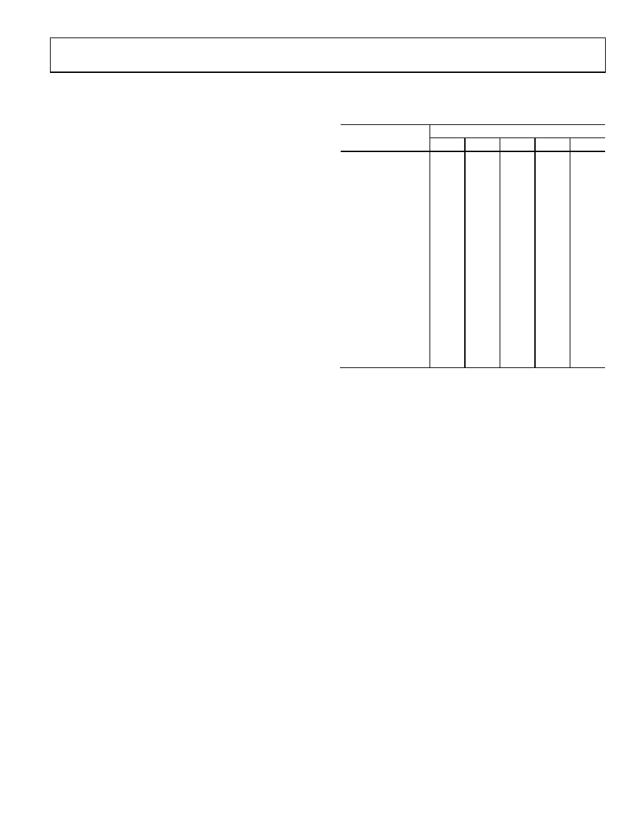
Table 8. REFCLK Multiplier Control Register Values
Reference Multiplier
Multiplier Value
Bit 4
Bit 3
Bit 2
Bit 1
Bit 0
4
0
1
0
5
0
1
0
1
6
0
1
0
7
0
1
8
0
1
0
9
0
1
0
1
10
0
1
0
1
0
11
0
1
0
1
12
0
1
0
13
0
1
0
1
14
0
1
0
15
0
1
16
1
0
17
1
0
1
18
1
0
1
0
19
1
0
1
20
1
0
1
0
SERIAL PORT I/O OPERATION
With the S/P SELECT pin tied low, the serial I/O mode is
active. The AD9852 serial port is a flexible, synchronous, serial
communication port, allowing easy interface to many industry-
standard microcontrollers and microprocessors. The serial I/O
is compatible with most synchronous transfer formats, including
both the Motorola 6905/11 SPI and Intel 8051 SSR protocols.
The interface allows read/write access to all 12 registers that
configure the AD9852 and can be configured as a single-pin
I/O (SDIO) or two unidirectional pins for input and output
(SDIO/SDO). Data transfers are supported in MSB- or LSB-
first format at up to 10 MHz.
When configured for serial I/O operation, most pins from the
AD9852 parallel port are inactive; only some pins are used for
serial I/O operation. Table 10 describes pin requirements for
serial I/O operation.
When operating the device in the serial I/O mode, it is best to
use the external I/O update clock mode to avoid an I/O update
clock occurring during a serial communication cycle. Such an
occurrence may cause incorrect programming due to a partial
data transfer. Therefore, users should write to the device between
I/O update clocks. To exit the default internal update mode,
program the device for external update operation at power-up
before starting the REFCLK signal but after a master reset.
Starting the REFCLK causes this information to transfer to the
register bank, forcing the device to switch to external update mode.
相关PDF资料 |
PDF描述 |
|---|---|
| AD9854ASTZ | IC DDS QUADRATURE CMOS 80-LQFP |
| AD9858BSVZ | IC DDS DAC 10BIT 1GSPS 100-TQFP |
| AD9859YSVZ-REEL7 | IC DDS DAC 10BIT 400MSPS 48TQFP |
| AD9880KSTZ-100 | IC INTERFACE/HDMI 100MHZ 100LQFP |
| AD9882KSTZ-140 | IC INTERFACE/DVI 100MHZ 100LQFP |
相关代理商/技术参数 |
参数描述 |
|---|---|
| AD9852ASVZ | 制造商:Analog Devices 功能描述:IC DDS 300MHz TQFP-80 制造商:Analog Devices 功能描述:IC, DDS, 300MHz, TQFP-80 |
| AD9852ASVZ1 | 制造商:AD 制造商全称:Analog Devices 功能描述:CMOS 300 MSPS Complete DDS |
| AD9852BSVZ | 制造商:Analog Devices 功能描述: |
| AD9853 | 制造商:AD 制造商全称:Analog Devices 功能描述:Programmable Digital OPSK/16-QAM Modulator |
| AD9853-45PCB | 制造商:AD 制造商全称:Analog Devices 功能描述:Programmable Digital OPSK/16-QAM Modulator |
发布紧急采购,3分钟左右您将得到回复。