参数资料
| 型号: | AD9974BBCZRL |
| 厂商: | Analog Devices Inc |
| 文件页数: | 25/52页 |
| 文件大小: | 0K |
| 描述: | IC CCDSP DUAL 14BIT 100-CSPBGA |
| 标准包装: | 1 |
| 类型: | CCD 信号处理器,14 位 |
| 输入类型: | 逻辑 |
| 输出类型: | 逻辑 |
| 接口: | 3 线串口 |
| 电流 - 电源: | 55mA |
| 安装类型: | 表面贴装 |
| 封装/外壳: | 100-LFBGA,CSPBGA |
| 供应商设备封装: | 100-CSBGA(9x9) |
| 包装: | 标准包装 |
| 其它名称: | AD9974BBCZRLDKR |
第1页第2页第3页第4页第5页第6页第7页第8页第9页第10页第11页第12页第13页第14页第15页第16页第17页第18页第19页第20页第21页第22页第23页第24页当前第25页第26页第27页第28页第29页第30页第31页第32页第33页第34页第35页第36页第37页第38页第39页第40页第41页第42页第43页第44页第45页第46页第47页第48页第49页第50页第51页第52页
AD9974
Rev. A | Page 31 of 52
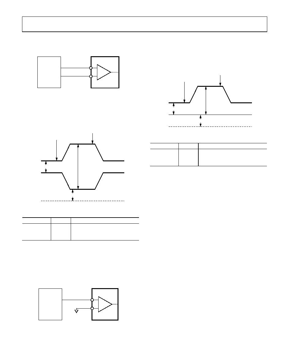
SHA Mode—Differential Input Configuration
This configuration uses a differential input sample/hold
amplifier (SHA) (see Figure 43).
IMAGE
SENSOR
SHA/
CDS
CCDINM
CCDINP
AD9974
05
95
5-
04
3
Figure 43. SHA Mode—Differential Input Configuration
In this configuration, a signal is applied to the CCDINP input
and, simultaneously, an inverse signal is applied to the CCDINM
input. Sampling occurs on both signals at the same time. This
creates the differential output for amplification and the ADC
(N + 1) SIGNAL SAMPLE
(N) SIGNAL SAMPLE
INPUT_POS
INPUT_NEG
PEAK SIGNAL
LEVEL (VFS)
BLACK SIGNAL LEVEL (VBLK)
MINIMUM SIGNAL LEVEL (VMIN)
GND
05
95
5-
04
4
Figure 44. SHA Mode—Differential Input Signal
Table 18. SHA Mode—Differential Voltage Levels
Signal Level
Symbol
Min (mV)
Typ (mV)
Max (mV)
Black
VBLK
0
Saturation
VFS
1000
VDD 300
1400
Minimum
VMIN
0
1800
SHA Mode—DC-Coupled, Single–Ended Input
The SHA mode can also be used in a single-ended fashion, with
the signal from the image sensor applied to the CDS/SHA using
a single input, CCDINP. This is similar to the differential configu-
ration, except in this case, the CCDINM line is held at a constant
dc voltage, establishing a reference level that matches the image
sensor reference voltage (see Figure 45).
IMAGE
SENSOR
SHA/
CDS
CCDINM
CCDINP
AD9974
NOTES
1. DC VOLTAGE ABOVE GROUND MAYBE USED TO
MATCH THE SENSOR REFERENCE LEVEL.
059
55
-04
5
Figure 45. SHA Mode—Single–Ended Input Configuration, DC-Coupled
constant dc voltage set at a level above ground potential. The
sensor signal is applied to the other input, and samples are taken
at the signal minimum and at a point of signal maximum. The
resulting differential signal is the difference between the signal
and the reference voltage.
(N + 1) SIGNAL SAMPLE
(N) SIGNAL SAMPLE
INPUT_POS
INPUT_NEG
PEAK SIGNAL
LEVEL (VFS)
BLACK SIGNAL LEVEL (VBLK)
MINIMUM SIGNAL LEVEL (VMIN)
GND
0
59
55
-04
6
Figure 46. SHA Mode—Single–Ended Input Signal (DC-Coupled)
Table 19. SHA Mode—Single-Ended Input Voltages
Signal Level
Symbol
Min (mV)
Typ (mV)
Max (mV)
Black
VBLK
0
Saturation
VFS
1000
1400
Minimum
VMIN
0
CDS Timing Control
The timing shown in Figure 21 illustrates how the two internally
generated CDS clocks, SHP and SHD, are used to sample the
reference level and data level of the CCD signal, respectively. The
placement of the SHP and SHD sampling edges is determined by
the setting of the SHPLOC and SHDLOC register located at
Address 0x36. Placement of these two clock signals is critical in
achieving the best performance from the CCD.
SHA Timing Control
When SHA mode is selected, only the SHPLOC setting is used
to sample the input signal, but the SHDLOC signal should still
be programmed to an edge setting of SHPLOC + 32.
相关PDF资料 |
PDF描述 |
|---|---|
| AD9979BCPZRL | IC PROCESSOR CCD 14BIT 48-LFCSP |
| AD9980KSTZ-95 | IC INTERFACE 8BIT ANALOG 80LQFP |
| AD9981KSTZ-95 | IC INTERFACE 10BIT ANALOG 80LQFP |
| AD9983AKSTZ-170 | IC DISPLAY 8BIT 170MSPS 80LQFP |
| AD9985KSTZ-140 | IC INTERFACE 8BIT 140MSPS 80LQFP |
相关代理商/技术参数 |
参数描述 |
|---|---|
| AD9975 | 制造商:AD 制造商全称:Analog Devices 功能描述:Broadband Modem Mixed-Signal Front End |
| AD9975ABST | 制造商:AD 制造商全称:Analog Devices 功能描述:Broadband Modem Mixed-Signal Front End |
| AD9975ABSTEB | 制造商:AD 制造商全称:Analog Devices 功能描述:Broadband Modem Mixed-Signal Front End |
| AD9975ABSTRL | 制造商:AD 制造商全称:Analog Devices 功能描述:Broadband Modem Mixed-Signal Front End |
| AD9975BST | 制造商:Analog Devices 功能描述:Mixed Signal Front End 48-Pin LQFP 制造商:Rochester Electronics LLC 功能描述:10 BIT ANALOG FRONT END WITH HALF DUPLEX - Tape and Reel |
发布紧急采购,3分钟左右您将得到回复。