- 您现在的位置:买卖IC网 > PDF目录9660 > ADN2818ACPZ-RL7 (Analog Devices Inc)IC CLOCK/DATA RECOVERY 32-LFCSP PDF资料下载
参数资料
| 型号: | ADN2818ACPZ-RL7 |
| 厂商: | Analog Devices Inc |
| 文件页数: | 11/40页 |
| 文件大小: | 0K |
| 描述: | IC CLOCK/DATA RECOVERY 32-LFCSP |
| 标准包装: | 1,500 |
| 类型: | 时钟和数据恢复(CDR),多路复用器 |
| PLL: | 是 |
| 主要目的: | SONET/SDH |
| 输入: | CML |
| 输出: | CML |
| 电路数: | 1 |
| 比率 - 输入:输出: | 1:2 |
| 差分 - 输入:输出: | 是/是 |
| 频率 - 最大: | 2.7GHz |
| 电源电压: | 3 V ~ 3.6 V |
| 工作温度: | -40°C ~ 85°C |
| 安装类型: | 表面贴装 |
| 封装/外壳: | 32-VFQFN 裸露焊盘,CSP |
| 供应商设备封装: | 32-LFCSP-VQ(5x5) |
| 包装: | 带卷 (TR) |
第1页第2页第3页第4页第5页第6页第7页第8页第9页第10页当前第11页第12页第13页第14页第15页第16页第17页第18页第19页第20页第21页第22页第23页第24页第25页第26页第27页第28页第29页第30页第31页第32页第33页第34页第35页第36页第37页第38页第39页第40页
Data Sheet
ADN2817/ADN2818
Rev. E | Page 19 of 40
JITTER SPECIFICATIONS
The ADN2817/ADN2818 CDR is designed to achieve the best
bit error rate (BER) performance and exceeds the jitter transfer,
generation, and tolerance specifications proposed for SONET/SDH
equipment defined in the Telcordia Technologies specification.
Jitter is the dynamic displacement of digital signal edges from
their long-term average positions, measured in unit intervals
(UI), where 1 UI = 1 bit period. Jitter on the input data can cause
dynamic phase errors on the recovered clock sampling edge. Jitter
on the recovered clock causes jitter on the retimed data.
The following sections briefly summarize the specifications
of jitter generation, transfer, and tolerance in accordance with
the Telcordia document (GR-253-CORE, Issue 3, September
2000) for the optical interface at the equipment level and the
ADN2817/ADN2818 performance with respect to those
specifications.
JITTER GENERATION
The jitter generation specification limits the amount of jitter
that can be generated by the device with no jitter and wander
applied at the input. For OC-48 devices, the band-pass filter
has a 12 kHz high-pass cutoff frequency with a roll-off of
20 dB/decade and a low-pass cutoff frequency of at least
20 MHz. The jitter generated must be less than 0.01 UI rms
and must be less than 0.1 UI p-p.
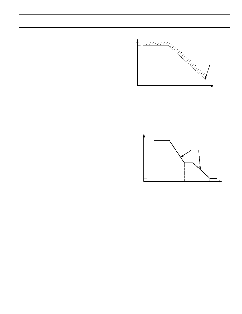
JITTER TRANSFER
The jitter transfer function is the ratio of the jitter on the output
signal to the jitter applied on the input signal vs. the frequency.
This parameter measures the limited amount of the jitter on
an input signal that can be transferred to the output signal
0.1
ACCEPTABLE
RANGE
fC
JITTER FREQUENCY (kHz)
SLOPE = –20dB/DECADE
JI
TTE
R
GA
IN
(
d
B
)
0
60
01-
01
5
Figure 26. Jitter Transfer Curve
JITTER TOLERANCE
The jitter tolerance is defined as the peak-to-peak amplitude of
the sinusoidal jitter applied on the input signal, which causes a
1 dB power penalty. This is a stress test intended to ensure that
no additional penalty is incurred under the operating conditions
(see Figure 27).
15.00
1.50
0.15
f0
f1
f2
f3
f4
JITTER FREQUENCY (kHz)
SLOPE = –20dB/DECADE
IN
P
U
T
J
ITT
E
R
A
M
P
L
ITU
D
E
(
U
I
p-
p
)
060
01
-01
6
Figure 27. SONET Jitter Tolerance Mask
相关PDF资料 |
PDF描述 |
|---|---|
| MS27472E24B35SA | CONN RCPT 128POS WALL MNT W/SCKT |
| MS27468T25B19P | CONN RCPT 19POS JAM NUT W/PINS |
| SY87701LZG | IC CLOCK/DATA RECOVERY 28-SOIC |
| VI-21Z-MV-F2 | CONVERTER MOD DC/DC 2V 60W |
| SY87721LHY TR | IC CLOCK/DATA RECOVERY 64-TQFP |
相关代理商/技术参数 |
参数描述 |
|---|---|
| ADN2819 | 制造商:AD 制造商全称:Analog Devices 功能描述:Multirate to 2.7 Gb/s Clock and Data Recovery IC with Integrated Limiting Amp |
| ADN2819ACP-CML | 制造商:Analog Devices 功能描述:CDR 2488.32Mbps/2666.06Mbps SONET/SDH 48-Pin LFCSP EP Tray 制造商:Rochester Electronics LLC 功能描述:MULTI-RATE 2.7GBPS CDR/ PA LOW POWER I.C - Bulk |
| ADN2819ACP-CML-RL | 制造商:Analog Devices 功能描述:CDR 2488.32Mbps/2666.06Mbps SONET/SDH 48-Pin LFCSP EP T/R |
| ADN2819ACPZ-CML | 功能描述:IC CLOCK/DATA RECOVERY 48LFCSP RoHS:是 类别:集成电路 (IC) >> 时钟/计时 - 专用 系列:- 标准包装:28 系列:- 类型:时钟/频率发生器 PLL:是 主要目的:Intel CPU 服务器 输入:时钟 输出:LVCMOS 电路数:1 比率 - 输入:输出:3:22 差分 - 输入:输出:无/是 频率 - 最大:400MHz 电源电压:3.135 V ~ 3.465 V 工作温度:0°C ~ 85°C 安装类型:表面贴装 封装/外壳:64-TFSOP (0.240",6.10mm 宽) 供应商设备封装:64-TSSOP 包装:管件 |
| ADN2819ACPZ-CML1 | 制造商:AD 制造商全称:Analog Devices 功能描述:Multirate to 2.7 Gb/s Clock and Data Recovery IC with Integrated Limiting Amp |
发布紧急采购,3分钟左右您将得到回复。