参数资料
| 型号: | ATMEGA103-6AI |
| 厂商: | Atmel |
| 文件页数: | 17/141页 |
| 文件大小: | 0K |
| 描述: | IC MCU 128K 6MHZ A/D IT 64TQFP |
| 产品培训模块: | megaAVR Introduction |
| 标准包装: | 90 |
| 系列: | AVR® ATmega |
| 核心处理器: | AVR |
| 芯体尺寸: | 8-位 |
| 速度: | 6MHz |
| 连通性: | SPI,UART/USART |
| 外围设备: | POR,PWM,WDT |
| 输入/输出数: | 32 |
| 程序存储器容量: | 128KB(64K x 16) |
| 程序存储器类型: | 闪存 |
| EEPROM 大小: | 4K x 8 |
| RAM 容量: | 4K x 8 |
| 电压 - 电源 (Vcc/Vdd): | 4 V ~ 5.5 V |
| 数据转换器: | A/D 8x10b |
| 振荡器型: | 内部 |
| 工作温度: | -40°C ~ 85°C |
| 封装/外壳: | 64-TQFP |
| 包装: | 托盘 |
| 配用: | ATSTK501-ND - ADAPTER KIT FOR 64PIN AVR MCU |
第1页第2页第3页第4页第5页第6页第7页第8页第9页第10页第11页第12页第13页第14页第15页第16页当前第17页第18页第19页第20页第21页第22页第23页第24页第25页第26页第27页第28页第29页第30页第31页第32页第33页第34页第35页第36页第37页第38页第39页第40页第41页第42页第43页第44页第45页第46页第47页第48页第49页第50页第51页第52页第53页第54页第55页第56页第57页第58页第59页第60页第61页第62页第63页第64页第65页第66页第67页第68页第69页第70页第71页第72页第73页第74页第75页第76页第77页第78页第79页第80页第81页第82页第83页第84页第85页第86页第87页第88页第89页第90页第91页第92页第93页第94页第95页第96页第97页第98页第99页第100页第101页第102页第103页第104页第105页第106页第107页第108页第109页第110页第111页第112页第113页第114页第115页第116页第117页第118页第119页第120页第121页第122页第123页第124页第125页第126页第127页第128页第129页第130页第131页第132页第133页第134页第135页第136页第137页第138页第139页第140页第141页
113
ATmega103(L)
0945I–AVR–02/07
Serial Downloading
Both the Flash and EEPROM memory arrays can be programmed using the serial inter-
face while RESET is pulled to GND, or when PEN is low during Power-on Reset. The
serial interface consists of pins SCK, RXD/PDI (input) and TXD/PDO (output). After
RESET is set low, the Programming Enable instruction needs to be executed first before
program/erase instructions can be executed.
For the EEPROM, an auto-erase cycle is provided within the self-timed Write instruction
and there is no need to first execute the Chip Erase instruction. The Chip Erase instruc-
tion turns the content of every memory location in both the Program and EEPROM
arrays into $FF.
The Program and EEPROM memory arrays have separate address spaces: $0000 to
$FFFF for Program memory and $0000 to $0FFF for EEPROM memory.
Either an external clock is supplied at pin XTAL1 or a crystal needs to be connected
across pins XTAL1 and XTAL2. The minimum low and high periods for the serial clock
(SCK) input are defined as follows:
Low: > 2 XTAL1 clock cycles
High: > 2 XTAL1 clock cycles
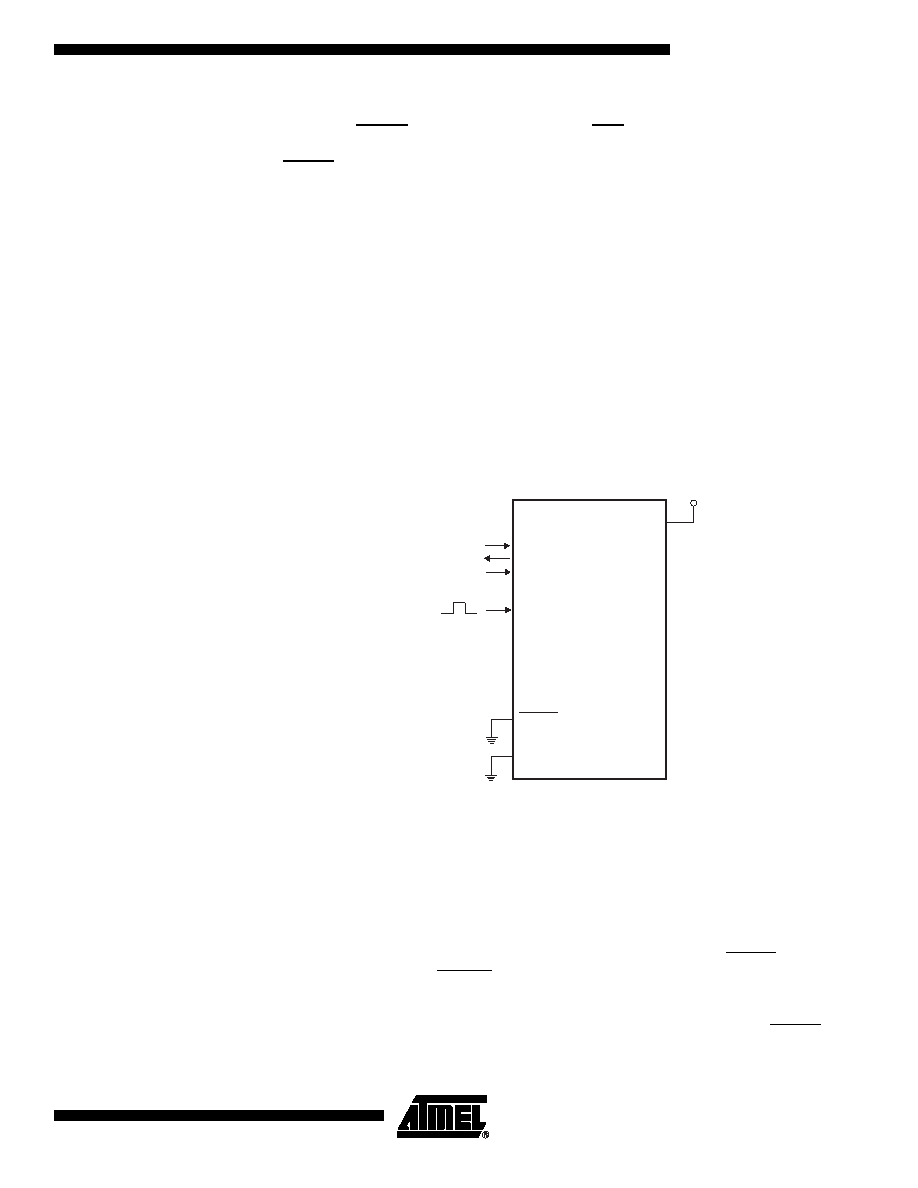
Figure 77. Serial Programming
Note:
Instruction in and data out is not using the SPI pins as on other AVR devices. SCK uses
the SPI pin as usual.
Serial Programming
Algorithm
When writing serial data to the ATmega103(L), data is sampled by the ATmega
103/103L on the rising edge of SCK. When reading data from the ATmega103(L), data
is clocked on the falling edge of SCK. See Figure 78 for an explanation. To program and
verify the ATmega103(L) in the Serial Programming mode, the following sequence is
recommended (See 4-byte instruction formats in Table 44.):
1.
Power-up sequence: Apply power between V
CC and GND while RESET and SCK
are set to “0”. The RESET signal must be kept low during the complete serial
programming session. If a crystal is not connected across pins XTAL1 and
XTAL2, apply a clock signal to the XTAL1 pin. In some systems, the programmer
cannot guarantee that SCK is held low during Power-up. In this case, RESET
must be given a positive pulse of at least two XTAL1 cycles duration after SCK
has been set to “0”.
ATmega103(L)
VCC
V
CC
PE0 (PD1/RXD)
PE1 (PD0/TXD)
PB1 (SCK)
RESET
GND
XTAL1
INSTR. IN
DATA OUT
CLOCK IN
相关PDF资料 |
PDF描述 |
|---|---|
| ATMEGA128A-AUR | MCU AVR 128K FLASH 16MHZ 64TQFP |
| ATMEGA128L-8MJ | IC MCU AVR 128K 8MHZ LV 64-QFN |
| ATMEGA16-16MUR | MCU AVR 16KB FLASH 16MHZ 44QFN |
| ATMEGA164PA-AN | IC MCU AVR 16K FLASH 44TQFP |
| ATMEGA164PA-CUR | MCU AVR 16KB FLASH 20MHZ 49VFBGA |
相关代理商/技术参数 |
参数描述 |
|---|---|
| ATMEGA103L | 制造商:ATMEL 制造商全称:ATMEL Corporation 功能描述:8-bit Microcontroller with 128K Bytes In-System Programmable Flash |
| ATMEGA103L-4AC | 功能描述:8位微控制器 -MCU TQFP-64 128K FLASH 3 RoHS:否 制造商:Silicon Labs 核心:8051 处理器系列:C8051F39x 数据总线宽度:8 bit 最大时钟频率:50 MHz 程序存储器大小:16 KB 数据 RAM 大小:1 KB 片上 ADC:Yes 工作电源电压:1.8 V to 3.6 V 工作温度范围:- 40 C to + 105 C 封装 / 箱体:QFN-20 安装风格:SMD/SMT |
| ATMEGA103L-4AI | 制造商:ATMEL 制造商全称:ATMEL Corporation 功能描述:8-Bit Microcontroller with 64K/128K Bytes In-System Programmable Flash |
| ATMEGA128 | 制造商:ATMEL 制造商全称:ATMEL Corporation 功能描述:8-bit Microcontroller with 128K Bytes In-System Programmable Flash |
| ATMEGA128(L) | 制造商:未知厂家 制造商全称:未知厂家 功能描述:ATmega128(L) Preliminary Summary [Updated 9/03. 23 Pages] |
发布紧急采购,3分钟左右您将得到回复。