参数资料
| 型号: | DS3106LN+ |
| 厂商: | Maxim Integrated Products |
| 文件页数: | 3/92页 |
| 文件大小: | 0K |
| 描述: | IC TIMING LINE CARD 64-LQFP |
| 产品培训模块: | Lead (SnPb) Finish for COTS Obsolescence Mitigation Program |
| 标准包装: | 160 |
| 类型: | 定时卡 IC,多路复用器 |
| PLL: | 是 |
| 主要目的: | 以太网,SONET/SDH,Stratum,电信 |
| 输入: | CMOS,TTL |
| 输出: | CMOS,LVDS,LVPECL,TTL |
| 电路数: | 1 |
| 比率 - 输入:输出: | 2:2 |
| 差分 - 输入:输出: | 无/是 |
| 频率 - 最大: | 312.5MHz |
| 电源电压: | 1.62 V ~ 1.98 V |
| 工作温度: | -40°C ~ 85°C |
| 安装类型: | 表面贴装 |
| 封装/外壳: | 64-LQFP |
| 供应商设备封装: | 64-LQFP(10x10) |
| 包装: | 托盘 |
| 产品目录页面: | 1429 (CN2011-ZH PDF) |
第1页第2页当前第3页第4页第5页第6页第7页第8页第9页第10页第11页第12页第13页第14页第15页第16页第17页第18页第19页第20页第21页第22页第23页第24页第25页第26页第27页第28页第29页第30页第31页第32页第33页第34页第35页第36页第37页第38页第39页第40页第41页第42页第43页第44页第45页第46页第47页第48页第49页第50页第51页第52页第53页第54页第55页第56页第57页第58页第59页第60页第61页第62页第63页第64页第65页第66页第67页第68页第69页第70页第71页第72页第73页第74页第75页第76页第77页第78页第79页第80页第81页第82页第83页第84页第85页第86页第87页第88页第89页第90页第91页第92页
DS3106
11
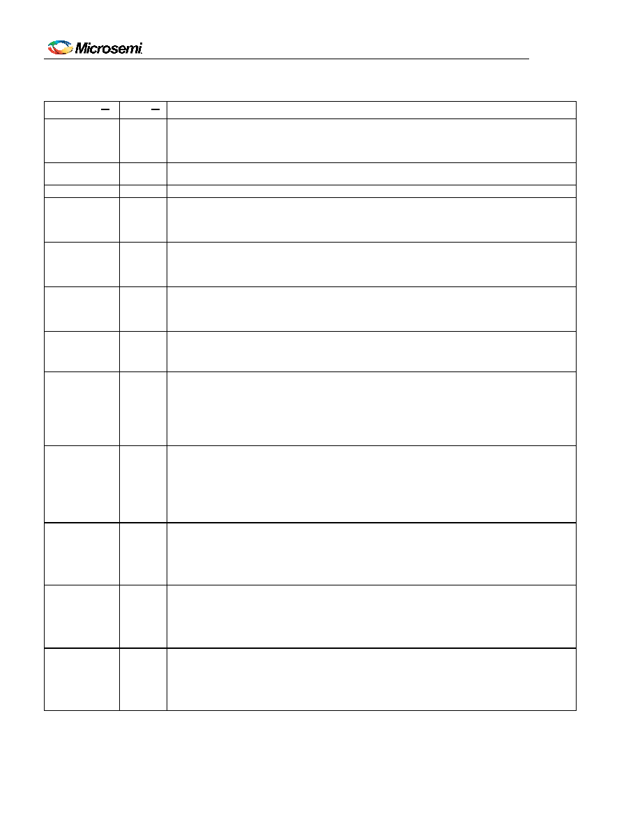
Table 6-3. Global Pin Descriptions
PIN NAME
TYPE
PIN DESCRIPTION
RST
IPU
Reset (Active Low). When this global asynchronous reset is pulled low, all internal circuitry is
reset to default values. The device is held in reset as long as
RST is low. RST should be held
low for at least two REFCLK cycles after the external oscillator has stabilized and is providing
valid clock signals.
SRCSW
IPD
Source Switching. Input reference selection pin. Selects IC3 when high and IC4 when low.
See Section 7.6.
TEST
IPD
Factory Test Mode Select. Wire this pin to VSS for normal operation.
IPF0
IPD
Input Frequency Select 0. Together with IPF1 and IPF2, this pin sets the default frequency of
the IC3 and IC4 input clock pins. The value is sampled when
RST goes high, and the
RST goes high this
pin is ignored.
IPF1
IPD
Input Frequency Select 1. Together with IPF0 and IPF2, this pin sets the default frequency of
the IC3 and IC4 input clock pins. The value is sampled when
RST goes high, and the
RST goes high this
pin is ignored.
IPF2
IPD
Input Frequency Select 2. Together with IPF0 and IPF1, this pin sets the default frequency of
the IC3 and IC4 input clock pins. The value is sampled when
RST goes high, and the
RST goes high this
pin is ignored.
O3F0
IPU
OC3 Frequency Select 0. This pin is sampled when the
RST pin goes high and the value is
used as O3F0, which, together with O3F2 and O3F1, sets the default frequency of the OC3
output clock pin. See Table 7-17. After
RST goes high this pin is ignored.
O3F1/SRFAIL
IOPU
OC3 Frequency Select 1/SRFAIL Status Pin. This pin is sampled when the
RST pin goes high
and the value is used as O3F1, which, together with O3F2 and O3F0, sets the default
frequency of the OC3 output clock pin. See Table 7-17. After
RST goes high, if MCR10:SRFPIN
= 1, this pin follows the state of the SRFAIL status bit in the MSR2 register. This gives the
system a very fast indication of the failure of the selected reference. When MCR10:SRFPIN = 0,
SRFAIL is disabled (high impedance).
O3F2/LOCK
IOPD
OC3 Frequency Select 2/T0 DPLL LOCK Status. This pin is sampled when the
RST pin goes
high and the value is used as O3F2, which, together with O3F1 and O3F0, sets the default
frequency of the OC3 output clock pin. See Table 7-17. After
RST goes high, if
0, LOCK is disabled (low).
0 = Not locked
1 = Locked
O6F0/GPIO1
IOPD
OC6 Frequency Select 0/General-Purpose I/O Pin 1. This pin is sampled when the
RST pin
goes high and the value is used as O6F0, which, together with O6F2 and O6F1, sets the
default frequency of the OC6 output clock pin. See Table 7-16. After
RST goes high, this pin
can be used as a general-purpose I/O pin. GPCR:GPIO1D configures this pin as an input or an
O6F1/GPIO2
IOPD
OC6 Frequency Select 1/General-Purpose I/O Pin 2. This pin is sampled when the
RST pin
goes high and the value is used as O6F1, which, together with O6F2 and O6F0, sets the
default frequency of the OC6 output clock pin. See Table 7-16. After
RST goes high, this pin
can be used as a general-purpose I/O pin. GPCR:GPIO2D configures this pin as an input or an
O6F2/GPIO3
IOPU
OC6 Frequency Select 2/General-Purpose I/O Pin 3. This pin is sampled when the
RST pin
goes high and the value is used as O6F2, which, together with O6F1 and O6F0, sets the
default frequency of the OC6 output clock pin. See Table 7-16. After
RST goes high, this pin
can be used as a general-purpose I/O pin. GPCR:GPIO3D configures this pin as an input or an
相关PDF资料 |
PDF描述 |
|---|---|
| DS3231MZ+ | IC RTC I2C 8SOIC |
| DS3231SN#T&R | IC RTC W/TCXO 16-SOIC |
| DS3232MZ+ | IC RTC W/SRAM I2C 8SOIC |
| DS3232SN#T&R | IC RTC W/TCXO 20-SOIC |
| DS3234S# | IC RTC W/TCXO 20-SOIC |
相关代理商/技术参数 |
参数描述 |
|---|---|
| DS3106LN+ | 功能描述:计时器和支持产品 Line Card Timing IC RoHS:否 制造商:Micrel 类型:Standard 封装 / 箱体:SOT-23 内部定时器数量:1 电源电压-最大:18 V 电源电压-最小:2.7 V 最大功率耗散: 最大工作温度:+ 85 C 最小工作温度:- 40 C 封装:Reel |
| DS3107FP000 | 制造商:Thomas & Betts 功能描述:30A,CON,2P3W,MG,107,125V |
| DS3107FRAB0 | 制造商:Thomas & Betts 功能描述:30A,REC,2P3W,MG,107,AB0,125,SC |
| DS3107MP000 | 制造商:Thomas & Betts 功能描述:30A,PLG,2P3W,MG,107,125V |
| DS3107MP00K | 制造商:Thomas & Betts 功能描述:30A,PLG,2P3W,MG,107,125V,CC |
发布紧急采购,3分钟左右您将得到回复。