参数资料
| 型号: | DS32512N# |
| 厂商: | Maxim Integrated Products |
| 文件页数: | 40/130页 |
| 文件大小: | 0K |
| 描述: | IC LIU DS3/E3/STS-1 484-BGA |
| 产品培训模块: | Lead (SnPb) Finish for COTS Obsolescence Mitigation Program |
| 标准包装: | 60 |
| 类型: | 线路接口装置(LIU) |
| 规程: | DS3 |
| 电源电压: | 3.135 V ~ 3.465 V |
| 安装类型: | 表面贴装 |
| 封装/外壳: | 484-BGA |
| 供应商设备封装: | 484-BGA(23x23) |
| 包装: | 管件 |
第1页第2页第3页第4页第5页第6页第7页第8页第9页第10页第11页第12页第13页第14页第15页第16页第17页第18页第19页第20页第21页第22页第23页第24页第25页第26页第27页第28页第29页第30页第31页第32页第33页第34页第35页第36页第37页第38页第39页当前第40页第41页第42页第43页第44页第45页第46页第47页第48页第49页第50页第51页第52页第53页第54页第55页第56页第57页第58页第59页第60页第61页第62页第63页第64页第65页第66页第67页第68页第69页第70页第71页第72页第73页第74页第75页第76页第77页第78页第79页第80页第81页第82页第83页第84页第85页第86页第87页第88页第89页第90页第91页第92页第93页第94页第95页第96页第97页第98页第99页第100页第101页第102页第103页第104页第105页第106页第107页第108页第109页第110页第111页第112页第113页第114页第115页第116页第117页第118页第119页第120页第121页第122页第123页第124页第125页第126页第127页第128页第129页第130页
DS32506/DS32508/DS32512
17 of 130
7.2 Detailed Pin Descriptions
n = port number (1 to 12 for DS32512, 1 to 8 for DS32508, 1 to 6 for DS32506). I = input, Ipu = input with internal pullup resistor, Ipd = input with
internal pulldown resistor, Ia = analog input, I/O = bidirectional in/out, I/Opd = bidirectional in/out with internal pulldown resistor, O = output, Oz =
high-impedance output (needs an external pullup or pulldown resistor to keep the node from floating), Oa = analog output (high impedance), P=
power supply or ground. All unused input pins without pullup should be tied low. Note: All internal pullup resistors are 50k
Ω tied to 2.2V DC.
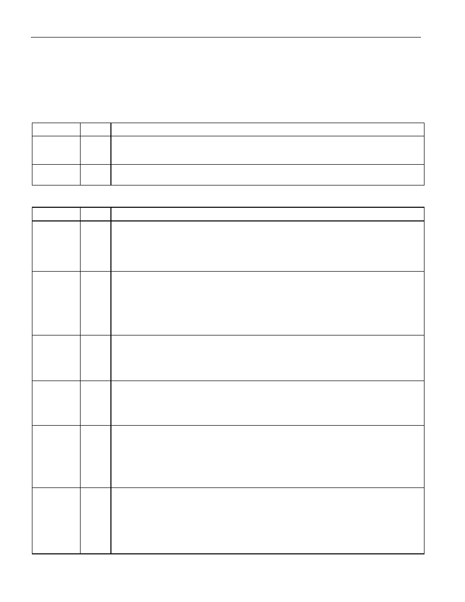
Table 7-2. Analog Line Interface Pin Descriptions
NAME
TYPE
FUNCTION
TXPn,
TXNn
Oa
Transmitter Analog Outputs. These differential AMI outputs are coupled to the outbound 75
Ω
coaxial cable through a 1:1 transformer (Figure 4-1). These outputs can be disabled (high
RXPn,
RXNn
Ia
Receiver Analog Inputs. These differential AMI inputs are coupled to the inbound 75
Ω coaxial
cable through a 1:1 transformer (Figure 4-1). See Section 8.3.1.
Table 7-3. Digital Framer Interface Pin Descriptions
NAME
TYPE
FUNCTION
TCLKn
I
Transmit Clock. A DS3 (44.736MHz
±20ppm), E3 (34.368MHz ±20ppm), or STS-1
(51.840MHz
±20ppm) clock should be applied at this pin. Data to be transmitted is clocked into
TCLKx (x
≠ 1) are ignored. See Section 8.2.1 for additional details.
TPOSn/
TDATn
I
Transmit Positive AMI/Transmit NRZ Data. This pin is sampled either on the rising edge of
pulse is transmitted on the line when TPOS is high.
TDAT is transmitted after B3ZS or HDB3 encoding.
TNEGn
I
Transmit Negative AMI. When the transmitter is configured to have a bipolar interface (TBIN =
0), a negative pulse is transmitted on the line when TNEG is high. When the transmitter is
RCLKn
Oz
Receive Clock. The clock recovered from the receive signal is output on the RCLK pin.
RPOSn/
RDATn
Oz
Receive Positive AMI/Receive NRZ Data. This pin is updated either on the falling edge of
high for each positive AMI pulse received.
decoded binary data.
RNEGn/
RLCVn
Oz
Receive Negative AMI/Receive Line-Code Violation. This pin is updated either on the falling
further details on code violations.
high for each negative AMI pulse received.
high to flag code violations.
相关PDF资料 |
PDF描述 |
|---|---|
| MAX1228AEEP+T | IC ADC 12BIT 300KSPS 20-QSOP |
| VI-26W-IU-F4 | CONVERTER MOD DC/DC 5.5V 200W |
| DS32512+ | IC LIU DS3/E3/STS-1 484-BGA |
| VI-26W-IU-F2 | CONVERTER MOD DC/DC 5.5V 200W |
| M83723/71W1020Y | CONN RCPT 2POS WALL MT W/SCKT |
相关代理商/技术参数 |
参数描述 |
|---|---|
| DS32512N# | 功能描述:网络控制器与处理器 IC 12-Port DS3/E3/STS-1 Line Interface Unit RoHS:否 制造商:Micrel 产品:Controller Area Network (CAN) 收发器数量: 数据速率: 电源电流(最大值):595 mA 最大工作温度:+ 85 C 安装风格:SMD/SMT 封装 / 箱体:PBGA-400 封装:Tray |
| DS32512N+ | 功能描述:网络控制器与处理器 IC 12-Port DS3/E3/STS-1 Line Interface Unit RoHS:否 制造商:Micrel 产品:Controller Area Network (CAN) 收发器数量: 数据速率: 电源电流(最大值):595 mA 最大工作温度:+ 85 C 安装风格:SMD/SMT 封装 / 箱体:PBGA-400 封装:Tray |
| DS32512NA2 | 制造商:Maxim Integrated Products 功能描述:DS32512 X12 DS3/E3 LIU REVA2 IND - Rail/Tube |
| DS32512NW | 功能描述:网络控制器与处理器 IC RoHS:否 制造商:Micrel 产品:Controller Area Network (CAN) 收发器数量: 数据速率: 电源电流(最大值):595 mA 最大工作温度:+ 85 C 安装风格:SMD/SMT 封装 / 箱体:PBGA-400 封装:Tray |
| DS32512W | 功能描述:网络控制器与处理器 IC RoHS:否 制造商:Micrel 产品:Controller Area Network (CAN) 收发器数量: 数据速率: 电源电流(最大值):595 mA 最大工作温度:+ 85 C 安装风格:SMD/SMT 封装 / 箱体:PBGA-400 封装:Tray |
发布紧急采购,3分钟左右您将得到回复。