参数资料
| 型号: | DS32512N# |
| 厂商: | Maxim Integrated Products |
| 文件页数: | 88/130页 |
| 文件大小: | 0K |
| 描述: | IC LIU DS3/E3/STS-1 484-BGA |
| 产品培训模块: | Lead (SnPb) Finish for COTS Obsolescence Mitigation Program |
| 标准包装: | 60 |
| 类型: | 线路接口装置(LIU) |
| 规程: | DS3 |
| 电源电压: | 3.135 V ~ 3.465 V |
| 安装类型: | 表面贴装 |
| 封装/外壳: | 484-BGA |
| 供应商设备封装: | 484-BGA(23x23) |
| 包装: | 管件 |
第1页第2页第3页第4页第5页第6页第7页第8页第9页第10页第11页第12页第13页第14页第15页第16页第17页第18页第19页第20页第21页第22页第23页第24页第25页第26页第27页第28页第29页第30页第31页第32页第33页第34页第35页第36页第37页第38页第39页第40页第41页第42页第43页第44页第45页第46页第47页第48页第49页第50页第51页第52页第53页第54页第55页第56页第57页第58页第59页第60页第61页第62页第63页第64页第65页第66页第67页第68页第69页第70页第71页第72页第73页第74页第75页第76页第77页第78页第79页第80页第81页第82页第83页第84页第85页第86页第87页当前第88页第89页第90页第91页第92页第93页第94页第95页第96页第97页第98页第99页第100页第101页第102页第103页第104页第105页第106页第107页第108页第109页第110页第111页第112页第113页第114页第115页第116页第117页第118页第119页第120页第121页第122页第123页第124页第125页第126页第127页第128页第129页第130页
DS32506/DS32508/DS32512
60 of 130
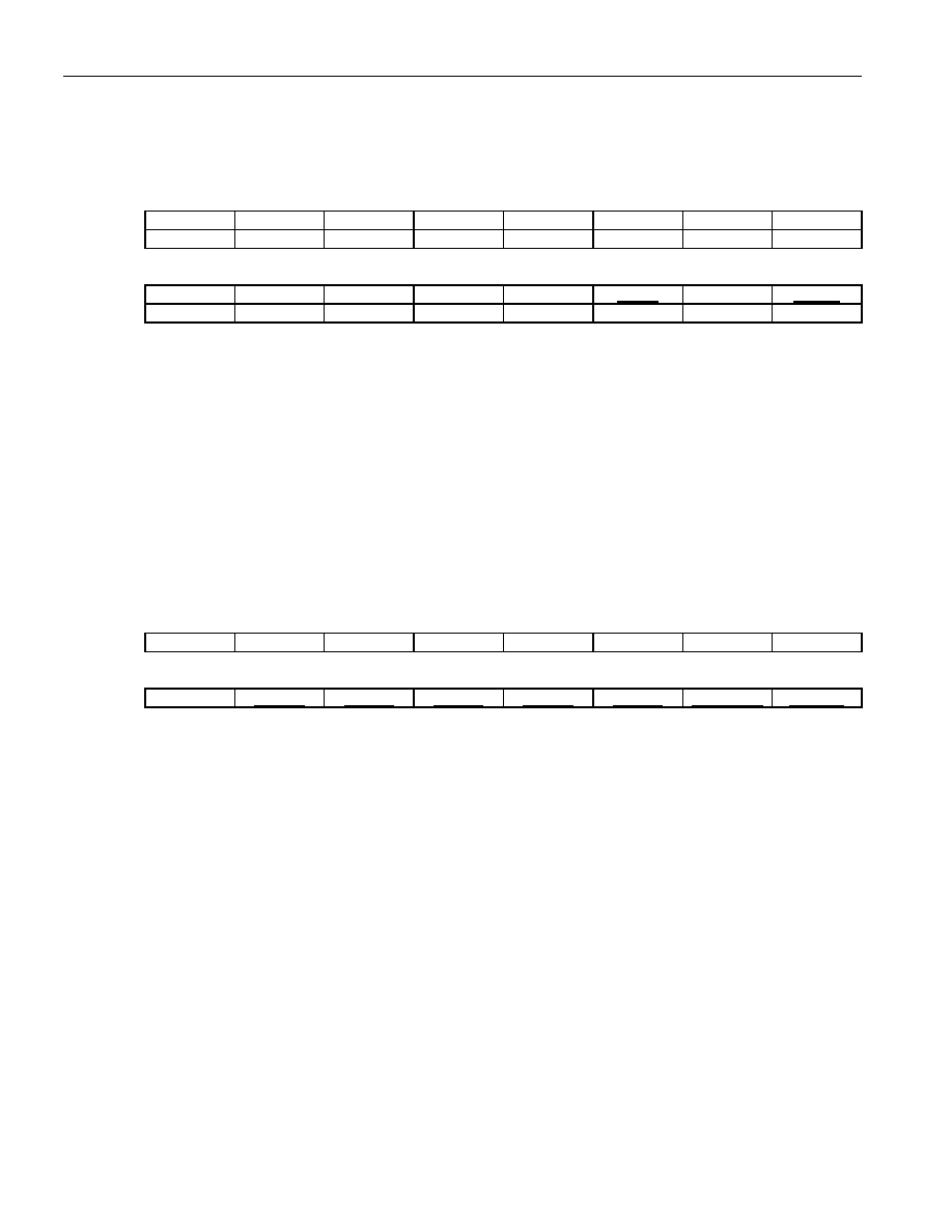
Register Name:
GLOBAL.SR
Register Description:
Global Status Register
Register Address:
028h
Bit #
15
14
13
12
11
10
9
8
Name
—
Default
—
Bit #
7
6
5
4
3
2
1
0
Name
—
CLOL
—
GPMS
Default
—
0
—
0
Bit 2: CLAD Loss of Lock (CLOL).
This bit is set when the CLAD is not locked to the reference frequency.
Bit 0: Global Performance Monitoring Update Status (GPMS).
This bit is set when the PORT.SR:PMS status
bits are set in all of the ports that are enabled for global update control (i.e., all ports that have PORT.CR1:PMUM =
1). Ports that have PORT.CR1:PMUM = 0 have no effect on this bit. In global software update mode, the global
update request bit (GLOBAL.CR1:GPMU) should be held high until this status bit goes high. See Section 8.7.4.
0 = The associated update request signal is low or not all register updates are completed.
1 = The requested performance register updates are all completed.
Register Name:
GLOBAL.SRL
Register Description:
Global Status Register Latched
Register Address:
02Ah
Bit #
15
14
13
12
11
10
9
8
Name
—
Bit #
7
6
5
4
3
2
1
0
Name
—
CLKCL
CLKBL
CLKAL
CLADL
CLOLL
G1SREFL
GPMSL
Bit 6: CLAD C Clock Activity Latched (CLKCL).
This bit is set when the signal on the CLKC pin is active. Note:
This bit should always be low when GLOBAL.CR2:CLAD[6:4]
≠ 000. See Section 8.7.1.
Bit 5: CLAD B Clock Activity Latched (CLKBL).
This bit is set when the signal on the CLKB pin is active. Note:
This bit should always be low when GLOBAL.CR2:CLAD[6:4]
≠ 000. See Section 8.7.1.
Bit 4: CLAD A Clock Activity Latched (CLKAL).
This bit is set when the signal on the CLKA pin is active. Note:
This bit should always be low when GLOBAL.CR2:CLAD[6:4]
≠ 000. See Section 8.7.1.
Bit 3: CLAD Reference Clock Activity Status Latched (CLADL).
This bit is set when the CLAD PLL reference
clock signal on the REFCLK pin is active. Note: When GLOBAL.CR2:CLAD[6:4] = 000, the REFCLK pin is unused.
See Section 8.7.1.
Bit 2: CLAD Loss of Lock Latched (CLOLL).
This bit is set when the GLOBAL.SR:CLOL status bit transitions
from low to high.
Bit 1: Global One-Second Status Latched (G1SREFL).
This bit is set once each second when the internal global
one-second timer signal transitions low to high. When set, this bit causes an interrupt if interrupt enables
Bit 0: Global Performance Monitoring Update Status Latched (GPMSL).
This bit is set when the
GLOBAL.SR:GPMS status bit changes from low to high. When set, this bit causes an interrupt if interrupt enables
相关PDF资料 |
PDF描述 |
|---|---|
| MAX1228AEEP+T | IC ADC 12BIT 300KSPS 20-QSOP |
| VI-26W-IU-F4 | CONVERTER MOD DC/DC 5.5V 200W |
| DS32512+ | IC LIU DS3/E3/STS-1 484-BGA |
| VI-26W-IU-F2 | CONVERTER MOD DC/DC 5.5V 200W |
| M83723/71W1020Y | CONN RCPT 2POS WALL MT W/SCKT |
相关代理商/技术参数 |
参数描述 |
|---|---|
| DS32512N# | 功能描述:网络控制器与处理器 IC 12-Port DS3/E3/STS-1 Line Interface Unit RoHS:否 制造商:Micrel 产品:Controller Area Network (CAN) 收发器数量: 数据速率: 电源电流(最大值):595 mA 最大工作温度:+ 85 C 安装风格:SMD/SMT 封装 / 箱体:PBGA-400 封装:Tray |
| DS32512N+ | 功能描述:网络控制器与处理器 IC 12-Port DS3/E3/STS-1 Line Interface Unit RoHS:否 制造商:Micrel 产品:Controller Area Network (CAN) 收发器数量: 数据速率: 电源电流(最大值):595 mA 最大工作温度:+ 85 C 安装风格:SMD/SMT 封装 / 箱体:PBGA-400 封装:Tray |
| DS32512NA2 | 制造商:Maxim Integrated Products 功能描述:DS32512 X12 DS3/E3 LIU REVA2 IND - Rail/Tube |
| DS32512NW | 功能描述:网络控制器与处理器 IC RoHS:否 制造商:Micrel 产品:Controller Area Network (CAN) 收发器数量: 数据速率: 电源电流(最大值):595 mA 最大工作温度:+ 85 C 安装风格:SMD/SMT 封装 / 箱体:PBGA-400 封装:Tray |
| DS32512W | 功能描述:网络控制器与处理器 IC RoHS:否 制造商:Micrel 产品:Controller Area Network (CAN) 收发器数量: 数据速率: 电源电流(最大值):595 mA 最大工作温度:+ 85 C 安装风格:SMD/SMT 封装 / 箱体:PBGA-400 封装:Tray |
发布紧急采购,3分钟左右您将得到回复。