参数资料
| 型号: | DS32512N# |
| 厂商: | Maxim Integrated Products |
| 文件页数: | 45/130页 |
| 文件大小: | 0K |
| 描述: | IC LIU DS3/E3/STS-1 484-BGA |
| 产品培训模块: | Lead (SnPb) Finish for COTS Obsolescence Mitigation Program |
| 标准包装: | 60 |
| 类型: | 线路接口装置(LIU) |
| 规程: | DS3 |
| 电源电压: | 3.135 V ~ 3.465 V |
| 安装类型: | 表面贴装 |
| 封装/外壳: | 484-BGA |
| 供应商设备封装: | 484-BGA(23x23) |
| 包装: | 管件 |
第1页第2页第3页第4页第5页第6页第7页第8页第9页第10页第11页第12页第13页第14页第15页第16页第17页第18页第19页第20页第21页第22页第23页第24页第25页第26页第27页第28页第29页第30页第31页第32页第33页第34页第35页第36页第37页第38页第39页第40页第41页第42页第43页第44页当前第45页第46页第47页第48页第49页第50页第51页第52页第53页第54页第55页第56页第57页第58页第59页第60页第61页第62页第63页第64页第65页第66页第67页第68页第69页第70页第71页第72页第73页第74页第75页第76页第77页第78页第79页第80页第81页第82页第83页第84页第85页第86页第87页第88页第89页第90页第91页第92页第93页第94页第95页第96页第97页第98页第99页第100页第101页第102页第103页第104页第105页第106页第107页第108页第109页第110页第111页第112页第113页第114页第115页第116页第117页第118页第119页第120页第121页第122页第123页第124页第125页第126页第127页第128页第129页第130页
DS32506/DS32508/DS32512
21 of 130
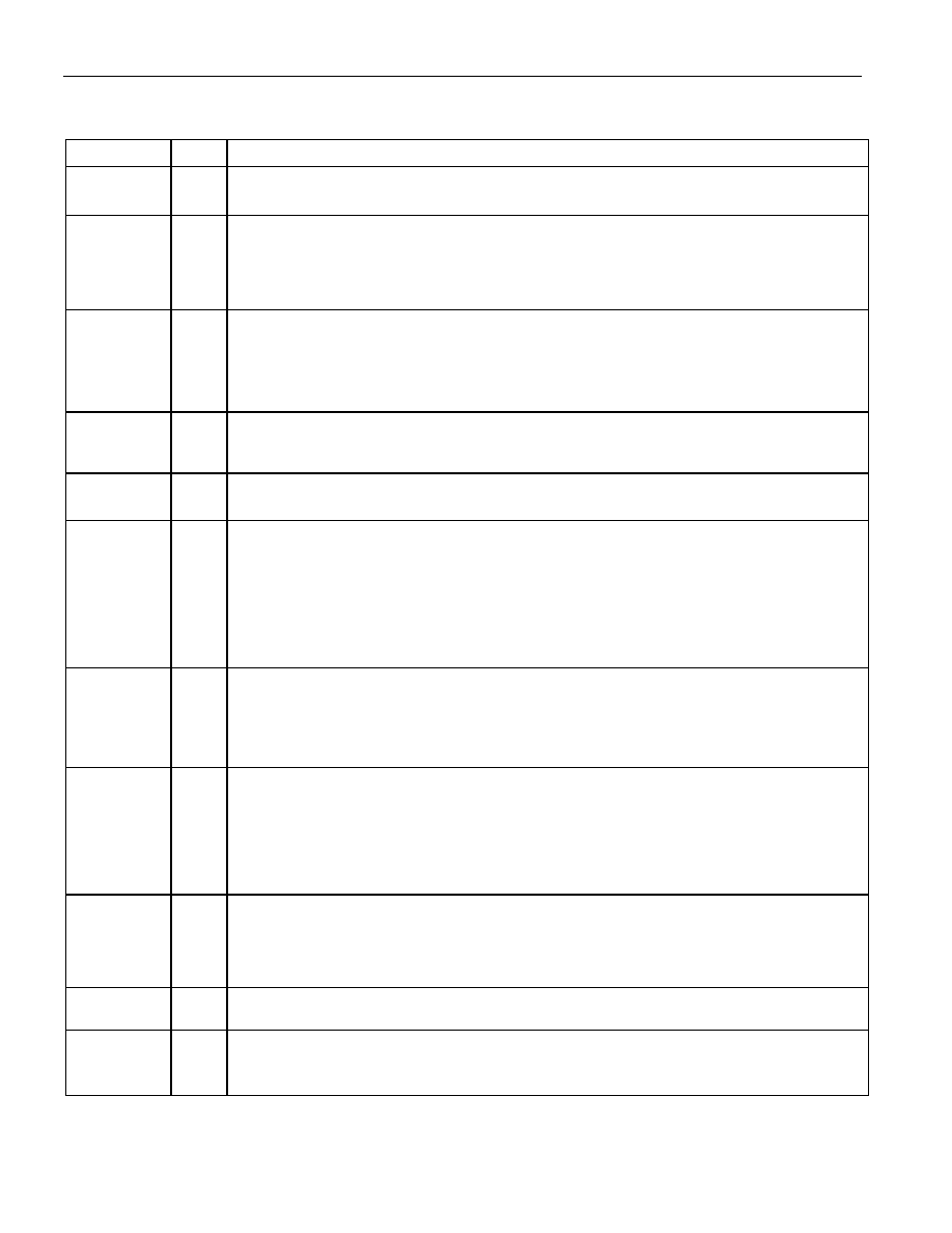
Table 7-6. Parallel Interface Pin Descriptions
NAME
TYPE
FUNCTION
CS
I
Chip Select (Active Low). This pin must be asserted to read or write internal registers. See
Section 8.8.3.
RD/DS
I
Read Enable (Active Low)/Data Strobe (Active Low)
WR/R/W
I
Write Enable (Active Low)/Read/Write Select
ALE
I
Address Latch Enable. This pin controls a latch on the A[10:0] inputs. For a nonmultiplexed
parallel bus, ALE is wired high to make the latch transparent. For a multiplexed parallel bus, the
falling edge of ALE latches the address. See Section 8.8.3.
A[10:1]
I
Address Bus (Excluding LSB). These inputs specify the address of the internal 16-bit register
to be accessed. A10 is not present on the DS32506. See Section 8.8.
A[0] /
BSWAP
I
Address Bus LSB/Byte Swap. See Section 8.8.2.
0 = Output register bits 7:0 on D[7:0]; D[15:8] high impedance
1 = Output register bits 15:8 on D[7:0]; D[15:8] high impedance
0 = Output register bits 15:8 on D[15:8] and bits 7:0 on D[7:0]
1 = Output register bits 7:0 on D[15:8] and bits 15:8 on D[7:0]
D[15:0]
I/O
Data Bus. A 8-bit or 16-bit bidirectional data bus. These pins are inputs during writes to internal
registers and outputs during reads. D[15:8] are disabled (high impedance) in 8-bit bus modes
(IFSEL = 10X). D[15:0] are disabled (high impedance) when
high. See Section 8.8.
RDY/
ACK
Oz
Ready Handshake (Tri-State)/Acknowledge Handshake (Tri-State, Active Low). Tri-stated
when
RDY: Intel Mode (IFSEL = 100 or 110): RDY goes high when the read or write cycle can
progress.
ACK: Motorola Mode (IFSEL = 101 or 111): ACK goes low when the read or write cycle can
progress.
INT
Oz
Interrupt Output (Active Low, Open Drain, or Push-Pull). This pin is driven low in response
to one or more unmasked, active interrupt sources within the device.
INT remains low until the
interrupt is serviced or masked. When GLOBAL.CR2:INTM = 0,
INT is high impedance when
inactive (default). When INTM = 1,
when
GPIOAn
I/Opd
General-Purpose I/O A. When a microprocessor interface is enabled (IFSEL
≠ 000), this pin is
the “A” general-purpose I/O pin for port n. See Section 8.7.3.
GPIOBn
I/Opd
General-Purpose I/O B. When a microprocessor interface is enabled (IFSEL
≠ 000), this pin is
the “B” general-purpose I/O pin for port n. See Section 8.7.3. Note: GPIOB1, GPIOB2, and
GPIOB3 can also be programmed as global control/status pins.
相关PDF资料 |
PDF描述 |
|---|---|
| MAX1228AEEP+T | IC ADC 12BIT 300KSPS 20-QSOP |
| VI-26W-IU-F4 | CONVERTER MOD DC/DC 5.5V 200W |
| DS32512+ | IC LIU DS3/E3/STS-1 484-BGA |
| VI-26W-IU-F2 | CONVERTER MOD DC/DC 5.5V 200W |
| M83723/71W1020Y | CONN RCPT 2POS WALL MT W/SCKT |
相关代理商/技术参数 |
参数描述 |
|---|---|
| DS32512N# | 功能描述:网络控制器与处理器 IC 12-Port DS3/E3/STS-1 Line Interface Unit RoHS:否 制造商:Micrel 产品:Controller Area Network (CAN) 收发器数量: 数据速率: 电源电流(最大值):595 mA 最大工作温度:+ 85 C 安装风格:SMD/SMT 封装 / 箱体:PBGA-400 封装:Tray |
| DS32512N+ | 功能描述:网络控制器与处理器 IC 12-Port DS3/E3/STS-1 Line Interface Unit RoHS:否 制造商:Micrel 产品:Controller Area Network (CAN) 收发器数量: 数据速率: 电源电流(最大值):595 mA 最大工作温度:+ 85 C 安装风格:SMD/SMT 封装 / 箱体:PBGA-400 封装:Tray |
| DS32512NA2 | 制造商:Maxim Integrated Products 功能描述:DS32512 X12 DS3/E3 LIU REVA2 IND - Rail/Tube |
| DS32512NW | 功能描述:网络控制器与处理器 IC RoHS:否 制造商:Micrel 产品:Controller Area Network (CAN) 收发器数量: 数据速率: 电源电流(最大值):595 mA 最大工作温度:+ 85 C 安装风格:SMD/SMT 封装 / 箱体:PBGA-400 封装:Tray |
| DS32512W | 功能描述:网络控制器与处理器 IC RoHS:否 制造商:Micrel 产品:Controller Area Network (CAN) 收发器数量: 数据速率: 电源电流(最大值):595 mA 最大工作温度:+ 85 C 安装风格:SMD/SMT 封装 / 箱体:PBGA-400 封装:Tray |
发布紧急采购,3分钟左右您将得到回复。