参数资料
| 型号: | DS32512N# |
| 厂商: | Maxim Integrated Products |
| 文件页数: | 47/130页 |
| 文件大小: | 0K |
| 描述: | IC LIU DS3/E3/STS-1 484-BGA |
| 产品培训模块: | Lead (SnPb) Finish for COTS Obsolescence Mitigation Program |
| 标准包装: | 60 |
| 类型: | 线路接口装置(LIU) |
| 规程: | DS3 |
| 电源电压: | 3.135 V ~ 3.465 V |
| 安装类型: | 表面贴装 |
| 封装/外壳: | 484-BGA |
| 供应商设备封装: | 484-BGA(23x23) |
| 包装: | 管件 |
第1页第2页第3页第4页第5页第6页第7页第8页第9页第10页第11页第12页第13页第14页第15页第16页第17页第18页第19页第20页第21页第22页第23页第24页第25页第26页第27页第28页第29页第30页第31页第32页第33页第34页第35页第36页第37页第38页第39页第40页第41页第42页第43页第44页第45页第46页当前第47页第48页第49页第50页第51页第52页第53页第54页第55页第56页第57页第58页第59页第60页第61页第62页第63页第64页第65页第66页第67页第68页第69页第70页第71页第72页第73页第74页第75页第76页第77页第78页第79页第80页第81页第82页第83页第84页第85页第86页第87页第88页第89页第90页第91页第92页第93页第94页第95页第96页第97页第98页第99页第100页第101页第102页第103页第104页第105页第106页第107页第108页第109页第110页第111页第112页第113页第114页第115页第116页第117页第118页第119页第120页第121页第122页第123页第124页第125页第126页第127页第128页第129页第130页
DS32506/DS32508/DS32512
23 of 130
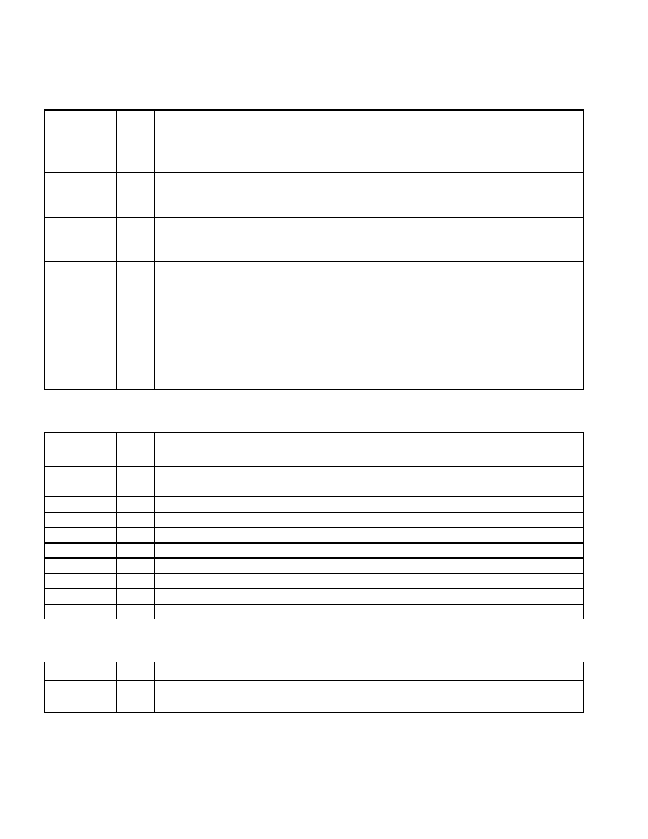
Table 7-9. JTAG Pin Descriptions
NAME
TYPE
FUNCTION
JTCLK
I
JTAG Clock. This pin shifts data into JTDI on the rising edge and out of JTDO on the
falling edge. JTCLK is typically a low frequency (less than 10MHz) 50% duty cycle clock
signal. If boundary scan is not used, JTCLK should be pulled high. See Section 10.
JTMS
Ipu
JTAG Mode Select. This pin is used to control the JTAG controller state machine. JTMS
is sampled on the rising edge of JTCLK. If boundary scan is not used, JTMS should be
left unconnected or pulled high. See Section 10.
JTDI
Ipu
JTAG Data Input. This pin is used to input data into the register that is enabled by the
JTAG controller state machine. JTDI is sampled on the rising edge of JTCLK. If boundary
scan is not used, JTDI should be left unconnected or pulled high. See Section 10.
JTDO
Oz
JTAG Data Output. This pin is the output of an internal scan shift register enabled by
the JTAG controller state machine. JTDO is updated on the falling edge of JTCLK. JTDO
is in high-impedance mode when a register is not selected or when the JTRST pin is low.
JTDO goes into and out of high-impedance mode after the falling edge of JTCLK. See
Section 10.
JTRST
Ipu
JTAG Reset (Active Low). When active, this pin forces the JTAG controller logic into
the reset state and forces the JTDO pin into high-impedance mode. The JTAG controller
is also reset when power is first applied via a power-on reset circuit. JTRST can be driven
high or low for normal operation, but must be high for JTAG operation. See Section 10.
Table 7-10. Power-Supply Pin Descriptions
NAME
TYPE
FUNCTION
VDD18
P
Digital Core 1.8V Power, 1.8V
±5%
VDD33
P
I/O 3.3V Power, 3.3V
±5%
VSS
P
Ground for VDD18 and VDD33
JVDDn
P
Jitter Attenuator 1.8V Power, 1.8V
±5%
JVSSn
P
Jitter Attenuator Ground
RVDDn
P
Receive 1.8V Power, 1.8V
±5%
RVSSn
P
Receive Ground
TVDDn
P
Transmit 1.8V Power, 1.8V
±5%
TVSSn
P
Transmit Ground
CVDD
P
CLAD 1.8V
±5%
CVSS
P
CLAD Ground
Table 7-11. Manufacturing Test Pin Descriptions
NAME
TYPE
FUNCTION
MT[10:0]
Test
Manufacturing Test Pins 10 to 0. MT[0] and MT[2:10] must not be connected. MT[1]
must be connected to digital ground (same as VSS pins).
相关PDF资料 |
PDF描述 |
|---|---|
| MAX1228AEEP+T | IC ADC 12BIT 300KSPS 20-QSOP |
| VI-26W-IU-F4 | CONVERTER MOD DC/DC 5.5V 200W |
| DS32512+ | IC LIU DS3/E3/STS-1 484-BGA |
| VI-26W-IU-F2 | CONVERTER MOD DC/DC 5.5V 200W |
| M83723/71W1020Y | CONN RCPT 2POS WALL MT W/SCKT |
相关代理商/技术参数 |
参数描述 |
|---|---|
| DS32512N# | 功能描述:网络控制器与处理器 IC 12-Port DS3/E3/STS-1 Line Interface Unit RoHS:否 制造商:Micrel 产品:Controller Area Network (CAN) 收发器数量: 数据速率: 电源电流(最大值):595 mA 最大工作温度:+ 85 C 安装风格:SMD/SMT 封装 / 箱体:PBGA-400 封装:Tray |
| DS32512N+ | 功能描述:网络控制器与处理器 IC 12-Port DS3/E3/STS-1 Line Interface Unit RoHS:否 制造商:Micrel 产品:Controller Area Network (CAN) 收发器数量: 数据速率: 电源电流(最大值):595 mA 最大工作温度:+ 85 C 安装风格:SMD/SMT 封装 / 箱体:PBGA-400 封装:Tray |
| DS32512NA2 | 制造商:Maxim Integrated Products 功能描述:DS32512 X12 DS3/E3 LIU REVA2 IND - Rail/Tube |
| DS32512NW | 功能描述:网络控制器与处理器 IC RoHS:否 制造商:Micrel 产品:Controller Area Network (CAN) 收发器数量: 数据速率: 电源电流(最大值):595 mA 最大工作温度:+ 85 C 安装风格:SMD/SMT 封装 / 箱体:PBGA-400 封装:Tray |
| DS32512W | 功能描述:网络控制器与处理器 IC RoHS:否 制造商:Micrel 产品:Controller Area Network (CAN) 收发器数量: 数据速率: 电源电流(最大值):595 mA 最大工作温度:+ 85 C 安装风格:SMD/SMT 封装 / 箱体:PBGA-400 封装:Tray |
发布紧急采购,3分钟左右您将得到回复。