- 您现在的位置:买卖IC网 > PDF目录1917 > DSPB56367AG150 (Freescale Semiconductor)IC DSP 24BIT 150MHZ 144-LQFP PDF资料下载
参数资料
| 型号: | DSPB56367AG150 |
| 厂商: | Freescale Semiconductor |
| 文件页数: | 79/100页 |
| 文件大小: | 0K |
| 描述: | IC DSP 24BIT 150MHZ 144-LQFP |
| 标准包装: | 60 |
| 系列: | DSP56K/Symphony |
| 类型: | 音频处理器 |
| 接口: | 主机接口,I²C,SAI,SPI |
| 时钟速率: | 150MHz |
| 非易失内存: | ROM(240 kB) |
| 芯片上RAM: | 69kB |
| 电压 - 输入/输出: | 3.30V |
| 电压 - 核心: | 1.80V |
| 工作温度: | -40°C ~ 95°C |
| 安装类型: | 表面贴装 |
| 封装/外壳: | 144-LQFP |
| 供应商设备封装: | 144-LQFP(20x20) |
| 包装: | 托盘 |
第1页第2页第3页第4页第5页第6页第7页第8页第9页第10页第11页第12页第13页第14页第15页第16页第17页第18页第19页第20页第21页第22页第23页第24页第25页第26页第27页第28页第29页第30页第31页第32页第33页第34页第35页第36页第37页第38页第39页第40页第41页第42页第43页第44页第45页第46页第47页第48页第49页第50页第51页第52页第53页第54页第55页第56页第57页第58页第59页第60页第61页第62页第63页第64页第65页第66页第67页第68页第69页第70页第71页第72页第73页第74页第75页第76页第77页第78页当前第79页第80页第81页第82页第83页第84页第85页第86页第87页第88页第89页第90页第91页第92页第93页第94页第95页第96页第97页第98页第99页第100页
Clock and PLL
DSP56367 Technical Data, Rev. 2.1
2-4
Freescale Semiconductor
2.4
Clock and PLL
2.5
External Memory Expansion Port (Port A)
When the DSP56367 enters a low-power standby mode (stop or wait), it releases bus mastership and
tri-states the relevant port A signals: A0–A17, D0–D23, AA0/RAS0–AA2/RAS2, RD, WR, BB, CAS.
2.6
External Address Bus
GNDC (2)
Bus Control Ground—GNDC is an isolated ground for the bus control I/O drivers. This connection must be
tied externally to all other chip ground connections. The user must provide adequate external decoupling
capacitors. There are two GNDC connections.
GNDH
Host Ground—GNDh is an isolated ground for the HD08 I/O drivers. This connection must be tied externally
to all other chip ground connections. The user must provide adequate external decoupling capacitors. There
is one GNDH connection.
GNDS (2)
SHI, ESAI, ESAI_1, DAX and Timer Ground—GNDS is an isolated ground for the SHI, ESAI, ESAI_1, DAX
and Timer. This connection must be tied externally to all other chip ground connections. The user must
provide adequate external decoupling capacitors. There are two GNDS connections.
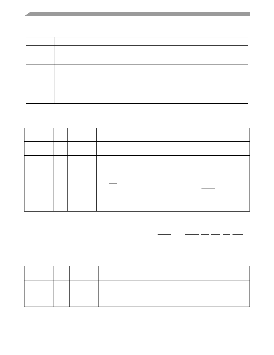
Table 2-4 Clock and PLL Signals
Signal Name
Type
State During
Reset
Signal Description
EXTAL
Input
External Clock Input—An external clock source must be connected to EXTAL in
order to supply the clock to the internal clock generator and PLL.
PCAP
Input
PLL Capacitor—PCAP is an input connecting an off-chip capacitor to the PLL filter.
Connect one capacitor terminal to PCAP and the other terminal to VCCP.
If the PLL is not used, PCAP may be tied to VCC, GND, or left floating.
PINIT/NMI
Input
PLL Initial/Nonmaskable Interrupt—During assertion of RESET, the value of
PINIT/NMI is written into the PLL Enable (PEN) bit of the PLL control register,
determining whether the PLL is enabled or disabled. After RESET de assertion and
during normal instruction processing, the PINIT/NMI Schmitt-trigger input is a
negative-edge-triggered nonmaskable interrupt (NMI) request internally synchronized
to internal system clock.
Table 2-5 External Address Bus Signals
Signal Name
Type
State During
Reset
Signal Description
A0–A17
Output
Tri-Stated
Address Bus—When the DSP is the bus master, A0–A17 are active-high outputs
that specify the address for external program and data memory accesses. Otherwise,
the signals are tri-stated. To minimize power dissipation, A0–A17 do not change state
when external memory spaces are not being accessed.
Table 2-3 Grounds (continued)
Ground Name
Description
相关PDF资料 |
PDF描述 |
|---|---|
| DSPB56371AF180 | IC DSP 24BIT 180MHZ 80-LQFP |
| DSPB56374AEC | IC DSP 24BIT 150MHZ 52-LQFP |
| DSPB56720CAG | DSP 24BIT AUD 200MHZ 144-LQFP |
| DSPB56724AG | DSP 24BIT AUD 250MHZ 144-LQFP |
| DSPIC30F2010T-20E/MM | IC DSPIC MCU/DSP 12K 28QFN |
相关代理商/技术参数 |
参数描述 |
|---|---|
| DSPB56367PV150 | 功能描述:数字信号处理器和控制器 - DSP, DSC 150Mhz/ 150MIPS RoHS:否 制造商:Microchip Technology 核心:dsPIC 数据总线宽度:16 bit 程序存储器大小:16 KB 数据 RAM 大小:2 KB 最大时钟频率:40 MHz 可编程输入/输出端数量:35 定时器数量:3 设备每秒兆指令数:50 MIPs 工作电源电压:3.3 V 最大工作温度:+ 85 C 封装 / 箱体:TQFP-44 安装风格:SMD/SMT |
| DSPB5636AG120 | 制造商:Freescale Semiconductor 功能描述: |
| DSPB56371AF150 | 功能描述:数字信号处理器和控制器 - DSP, DSC 150 MHZ VERSION DSPB371 RoHS:否 制造商:Microchip Technology 核心:dsPIC 数据总线宽度:16 bit 程序存储器大小:16 KB 数据 RAM 大小:2 KB 最大时钟频率:40 MHz 可编程输入/输出端数量:35 定时器数量:3 设备每秒兆指令数:50 MIPs 工作电源电压:3.3 V 最大工作温度:+ 85 C 封装 / 箱体:TQFP-44 安装风格:SMD/SMT |
| DSPB56371AF180 | 功能描述:数字信号处理器和控制器 - DSP, DSC BLANK ROM VERSION 56371 RoHS:否 制造商:Microchip Technology 核心:dsPIC 数据总线宽度:16 bit 程序存储器大小:16 KB 数据 RAM 大小:2 KB 最大时钟频率:40 MHz 可编程输入/输出端数量:35 定时器数量:3 设备每秒兆指令数:50 MIPs 工作电源电压:3.3 V 最大工作温度:+ 85 C 封装 / 箱体:TQFP-44 安装风格:SMD/SMT |
| DSPB56371AF180 | 制造商:Freescale Semiconductor 功能描述:Digital Signal Processor (DSP) IC |
发布紧急采购,3分钟左右您将得到回复。