- 您现在的位置:买卖IC网 > PDF目录15530 > EVAL-ADUC7039QSPZ (Analog Devices Inc)BOARD EVAL FOR ADUC7039 PDF资料下载
参数资料
| 型号: | EVAL-ADUC7039QSPZ |
| 厂商: | Analog Devices Inc |
| 文件页数: | 41/92页 |
| 文件大小: | 0K |
| 描述: | BOARD EVAL FOR ADUC7039 |
| 设计资源: | ADuC7039QSPZ Gerber Files EVAL-ADuC7039 Schematic & Brd Outline |
| 标准包装: | 1 |
| 系列: | QuickStart™ PLUS 套件 |
| 类型: | MCU |
| 适用于相关产品: | ADuC7039 |
| 所含物品: | 板 |
第1页第2页第3页第4页第5页第6页第7页第8页第9页第10页第11页第12页第13页第14页第15页第16页第17页第18页第19页第20页第21页第22页第23页第24页第25页第26页第27页第28页第29页第30页第31页第32页第33页第34页第35页第36页第37页第38页第39页第40页当前第41页第42页第43页第44页第45页第46页第47页第48页第49页第50页第51页第52页第53页第54页第55页第56页第57页第58页第59页第60页第61页第62页第63页第64页第65页第66页第67页第68页第69页第70页第71页第72页第73页第74页第75页第76页第77页第78页第79页第80页第81页第82页第83页第84页第85页第86页第87页第88页第89页第90页第91页第92页
ADuC7039
Data Sheet
Rev. D | Page 46 of 92
Understanding the Offset and Gain Calibration Registers
The output of the average block in the ADC signal flow can
be considered a fractional number with a span for a ±full-scale
input of approximately ±0.75. The span is less than ±1.0 because
there is attenuation in the modulator to accommodate some
overrange capacity on the input signal. The exact value of the
attenuation varies slightly from part-to-part because of
manufacturing tolerances.
The offset coefficient is read from the ADC0OF calibration
register. This value is a 16-bit, twos complement number. The
range of this number, in terms of the signal chain, is effectively
±1.0. Therefore, 1 LSB of the ADC0OF register is not the same
as 1 LSB of ADC0DAT.
A positive value of ADC0OF indicates that when offset is
subtracted from the output of the filter, a negative value is
added. The nominal value of this register is 0x0000, indicating
zero offset is to be removed. The actual offset of the ADC can
vary slightly from part-to-part and at different PGA gains. The
offset within the ADC is minimized if the chopping mode is
active (ADCFLT[15] = 1).
The gain coefficient is a unitless scaling factor. The 16-bit value
in this register is divided by 16,384 and then multiplied by the
offset corrected value. The nominal value of this register equals
0x5555, corresponding to a multiplication factor of 1.3333. This
scales the nominal ±0.75 signal to produce a full-scale output
signal of ±1.0 which is checked for overflow/underflow and
converted to twos complement or unipolar mode, as appro-
priate, before being output to the data register.
The actual gain, and the required scaling coefficient for zero
gain error, varies slightly from part to part and at different PGA
settings. The value downloaded into ADC0GN at power-on-
reset represents the scaling factor for a PGA gain = 4. There is
some level of gain error if this value is used at different PGA
settings. User code can run ADC calibrations and overwrite the
calibration coefficients to correct the gain error at the current
PGA setting.
In summary, the simplified ADC transfer function can be
described as
NOM
REF
IN
OUT
ADCGN
ADCOF
V
PGA
V
ADC
×
×
=
This equation is valid for the voltage/temperature channel ADC.
For the current channel ADC,
NOM
REF
IN
OUT
ADCGN
ADCOF
K
V
PGA
V
ADC
×
=
×
where K is dependent on the PGA gain setting and ADC mode.
For PGA gains of 4 and 32, the K factor is 1. For a PGA gain of
512, the K factor is 8.
ADC CONFIGURATION
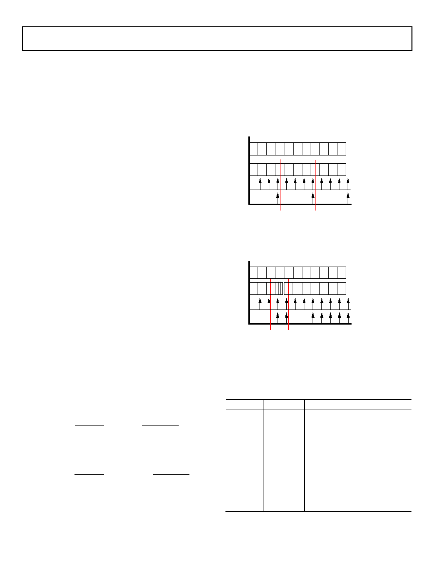
Fast Temperature Conversion Mode
The battery temperature can be derived through the on-chip
temperature sensor. By default, the time to a first valid (fully
settled) result after switching the ADC input from the voltage
to the temperature channel or from the temperature to the
voltage channel is three ADC conversion cycles with chop
mode turned off as shown in Figure 17.
Figure 17. Default Temperature Mode, Chop Off
A fast mode is provided on the temperature channel to
minimize the switching delay between voltage conversion and
temperature conversions as shown in Figure 18 and in Table 36.
Figure 18. Fast Temperature Mode, Chop Off ( ADCFLT = 0x07)
A request for a fast temperature conversion is executed with a
delay of one ADC conversion. The fast temperature mode must
be cleared after the temperature measurement is available but
before a new temperature request.
Table 36. Fast Temperature Mode
Interrupt
Valid Flags
User code
1
I and V
Voltage = ADC1DAT.
2
I and V
Voltage = ADC1DAT.
Set fast temperature request bit.
3
I and V
Voltage = ADC1DAT.
This data must be read for the next
temperature channel flag to be valid.
4
I and T
Temperature = ADC1DAT.
Clear fast temperature request bit.
5
I
6
I
7
I and V
Voltage = ADC1DAT.
8
I and V
Voltage = ADC1DAT.
VALID V/T
CONVERSION
V/T-ADC
SAMPLING
I-ADC
SAMPLING
I-ADC
INTERRUPT
V
T
CHANNEL SWITCHING REQUEST
V
T
08463-
031
V
T
VALID V/T
CONVERSION
V/T-ADC
SAMPLING
I-ADC
SAMPLING
I-ADC
INTERRUPT
CHANNEL SWITCHING REQUEST
V
08463-
032
相关PDF资料 |
PDF描述 |
|---|---|
| EYM15DRSH | CONN EDGECARD 30POS DIP .156 SLD |
| AIUR-06-102K | INDUCTOR POWER 1000UH 10% T/H |
| V300C3V3C50B2 | CONVERTER MOD DC/DC 3.3V 50W |
| EGM15DRSH | CONN EDGECARD 30POS DIP .156 SLD |
| EVAL-ADUC7023QSPZ1 | BOARD EVAL FOR ADUC7023 |
相关代理商/技术参数 |
参数描述 |
|---|---|
| EVAL-ADUC7060QSPZ | 功能描述:KIT DEV QUICK START ADUC7060 RoHS:是 类别:编程器,开发系统 >> 通用嵌入式开发板和套件(MCU、DSP、FPGA、CPLD等) 系列:QuickStart™ PLUS 套件 产品培训模块:Blackfin® Processor Core Architecture Overview Blackfin® Device Drivers Blackfin® Optimizations for Performance and Power Consumption Blackfin® System Services 特色产品:Blackfin? BF50x Series Processors 标准包装:1 系列:Blackfin® 类型:DSP 适用于相关产品:ADSP-BF548 所含物品:板,软件,4x4 键盘,光学拨轮,QVGA 触摸屏 LCD 和 40G 硬盘 配用:ADZS-BFBLUET-EZEXT-ND - EZ-EXTENDER DAUGHTERBOARDADZS-BFLLCD-EZEXT-ND - BOARD EXT LANDSCAP LCD INTERFACE 相关产品:ADSP-BF542BBCZ-4A-ND - IC DSP 16BIT 400MHZ 400CSBGAADSP-BF544MBBCZ-5M-ND - IC DSP 16BIT 533MHZ MDDR 400CBGAADSP-BF542MBBCZ-5M-ND - IC DSP 16BIT 533MHZ MDDR 400CBGAADSP-BF542KBCZ-6A-ND - IC DSP 16BIT 600MHZ 400CSBGAADSP-BF547MBBCZ-5M-ND - IC DSP 16BIT 533MHZ MDDR 400CBGAADSP-BF548BBCZ-5A-ND - IC DSP 16BIT 533MHZ 400CSBGAADSP-BF547BBCZ-5A-ND - IC DSP 16BIT 533MHZ 400CSBGAADSP-BF544BBCZ-5A-ND - IC DSP 16BIT 533MHZ 400CSBGAADSP-BF542BBCZ-5A-ND - IC DSP 16BIT 533MHZ 400CSBGA |
| EVAL-ADUC7060QSPZU1 | 制造商:Analog Devices 功能描述: |
| EVALADUC7060QSPZU2 | 制造商:Analog Devices 功能描述:QUICK START DEVELOPMENT SYSTEM - Boxed Product (Development Kits) |
| EVAL-ADUC7061MKZ | 功能描述:开发板和工具包 - ARM Quick Start Development System RoHS:否 制造商:Arduino 产品:Development Boards 工具用于评估:ATSAM3X8EA-AU 核心:ARM Cortex M3 接口类型:DAC, ICSP, JTAG, UART, USB 工作电源电压:3.3 V |
| EVAL-ADUC7061MKZ | 制造商:Analog Devices 功能描述:ADUC7061MKZ EvaluationBoard |
发布紧急采购,3分钟左右您将得到回复。