- 您现在的位置:买卖IC网 > PDF目录10950 > IDT821054PQFG (IDT, Integrated Device Technology Inc)IC PCM CODEC QUAD MPI 64-PQFP PDF资料下载
参数资料
| 型号: | IDT821054PQFG |
| 厂商: | IDT, Integrated Device Technology Inc |
| 文件页数: | 18/45页 |
| 文件大小: | 0K |
| 描述: | IC PCM CODEC QUAD MPI 64-PQFP |
| 标准包装: | 84 |
| 类型: | PCM 编解码器/滤波器 |
| 数据接口: | PCM 音频接口 |
| ADC / DAC 数量: | 4 / 4 |
| 三角积分调变: | 无 |
| 电压 - 电源,模拟: | 4.75 V ~ 5.25 V |
| 电压 - 电源,数字: | 4.75 V ~ 5.25 V |
| 工作温度: | -40°C ~ 85°C |
| 安装类型: | 表面贴装 |
| 封装/外壳: | 64-QFP |
| 供应商设备封装: | 64-PQFP(14x14) |
| 包装: | 管件 |
| 其它名称: | 800-2516-5 821054PQFG IDT821054PQFG-ND |
第1页第2页第3页第4页第5页第6页第7页第8页第9页第10页第11页第12页第13页第14页第15页第16页第17页当前第18页第19页第20页第21页第22页第23页第24页第25页第26页第27页第28页第29页第30页第31页第32页第33页第34页第35页第36页第37页第38页第39页第40页第41页第42页第43页第44页第45页
25
IDT821054 QUAD PROGRAMMABLE PCM CODEC WITH MPI INTERFACE
INDUSTRIAL TEMPERATURE RANGE
CHclk1[3:0] = 1000:
chclk1 outputs a digital signal with the frequency of 1000/16 Hz;
CHclk1[3:0] = 1001:
chclk1 outputs a digital signal with the frequency of 1000/18 Hz;
CHclk1[3:0] = 1010:
chclk1 outputs a digital signal with the frequency of 1000/20 Hz;
CHclk1[3:0] = 1011:
chclk1 outputs a digital signal with the frequency of 1000/22 Hz;
CHclk1[3:0] = 1100:
chclk1 outputs a digital signal with the frequency of 1000/24 Hz;
CHclk1[3:0] = 1101:
chclk1 outputs a digital signal with the frequency of 1000/26 Hz;
CHclk1[3:0] = 1110:
chclk1 outputs a digital signal with the frequency of 1000/28 Hz;
CHclk1[3:0] = 1111:
the output of chclk1 is set to low permanently.
GREG6: MCLK Selection and Channel Program Enable, Read/Write (25H/A5H)
The higher 4 bits (CE[3:0]) in this register are used to specify the desired channel(s) before addressing local registers or Coe-RAM. The
CE[0] to CE[3] bits indicate the program enable state for Channel 1 to Channel 4 respectively.
CE[0] = 0:
Disabled, Channel 1 can not receive programming commands (default);
CE[0] = 1:
Enabled, Channel 1 can receive programming commands;
CE[1] = 0:
Disabled, Channel 2 can not receive programming commands (default);
CE[1] = 1:
Enabled, Channel 2 can receive programming commands;
CE[2] = 0:
Disabled, Channel 3 can not receive programming commands (default);
CE[2] = 1:
Enabled, Channel 3 can receive programming commands;
CE[3] = 0:
Disabled, Channel 4 can not receive programming commands (default);
CE[3] = 1:
Enabled, Channel 4 can receive programming commands.
The lower 4 bits (Sel[3:0]) in this register are used to select the Master Clock frequency.
Sel[3:0] = 0000:
8.192 MHz
Sel[3:0] = 0001:
4.096 MHz
Sel[3:0] = 0010:
2.048 MHz (default)
Sel[3:0] = 0110:
1.536 MHz
Sel[3:0] = 1110:
1.544 MHz
Sel[3:0] = 0101:
3.072 MHz
Sel[3:0] = 1101:
3.088 MHz
Sel[3:0] = 0100:
6.144 MHz
Sel[3:0] = 1100:
6.176 MHz
GREG7: A/-law, Linear/Compressed Code, Clock Slope and Delay Time Selection, Read/Write (26H/A6H)
The A/-law select bit (A-) selects the companding law:
A- = 0:
A-law is selected (default)
A- = 1:
-law is selected.
The Voice Data Select bit (VDS) defines the format of the voice data:
VDS = 0:
Compressed code (default)
VDS = 1:
Linear code
The Clock Slope bits (CS[2:0]) select single or double clock and clock edges of transmitting and receiving data.
CS[2] = 0:
Single clock (default)
CS[2] = 1:
Double clock
CS[1:0] = 00:
transmits data on rising edges of BCLK, receives data on falling edges of BCLK (default).
CS[1:0] = 01:
transmits data on rising edges of BCLK, receives data on rising edges of BCLK.
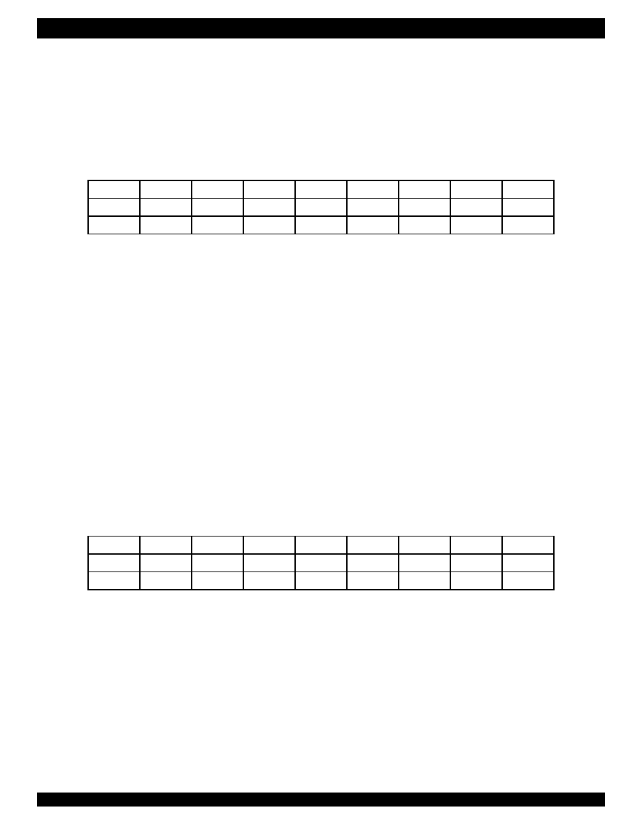
b7
b6
b5
b4
b3
b2
b1
b0
Command
R/W
0
1001
01
I/O data
CE[3]
CE[2]
CE[1]
CE[0]
Sel[3]
Sel[2]
Sel[1]
Sel[0]
b7
b6
b5
b4
b3
b2
b1
b0
Command
R/W
0
1001
10
I/O data
A-
VDS
CS[2]
CS[1]
CS[0]
OC[2]
OC[1]
OC[0]
相关PDF资料 |
PDF描述 |
|---|---|
| MCIMX357CVM5BR2 | IC MPU I.MX35 400MAPBGA |
| MCIMX357CVM5B | IC MPU I.MX35 400MAPBGA |
| MCIMX357CJQ5CR2 | MULTIMEDIA PROCESSOR 400-MAPBGA |
| MCF5270CVM150J | IC MCU 32BIT 150MHZ 196-MAPBGA |
| ADV202BBCZ-150 | IC VIDEO CODEC JPEG2000 144CSBGA |
相关代理商/技术参数 |
参数描述 |
|---|---|
| IDT821064 | 制造商:IDT 制造商全称:Integrated Device Technology 功能描述:QUAD PROGRAMMABLE PCM CODEC WITH GCI INTERFACE |
| IDT821064PQF | 制造商:IDT 制造商全称:Integrated Device Technology 功能描述:QUAD PROGRAMMABLE PCM CODEC WITH GCI INTERFACE |
| IDT821068 | 制造商:IDT 制造商全称:Integrated Device Technology 功能描述:OCTAL PROGRAMMABLE PCM CODEC |
| IDT821068PX | 制造商:IDT 制造商全称:Integrated Device Technology 功能描述:OCTAL PROGRAMMABLE PCM CODEC |
| IDT821621 | 制造商:IDT 制造商全称:Integrated Device Technology 功能描述:LONG HAUL SLIC |
发布紧急采购,3分钟左右您将得到回复。