- 您现在的位置:买卖IC网 > PDF目录10950 > IDT821054PQFG (IDT, Integrated Device Technology Inc)IC PCM CODEC QUAD MPI 64-PQFP PDF资料下载
参数资料
| 型号: | IDT821054PQFG |
| 厂商: | IDT, Integrated Device Technology Inc |
| 文件页数: | 43/45页 |
| 文件大小: | 0K |
| 描述: | IC PCM CODEC QUAD MPI 64-PQFP |
| 标准包装: | 84 |
| 类型: | PCM 编解码器/滤波器 |
| 数据接口: | PCM 音频接口 |
| ADC / DAC 数量: | 4 / 4 |
| 三角积分调变: | 无 |
| 电压 - 电源,模拟: | 4.75 V ~ 5.25 V |
| 电压 - 电源,数字: | 4.75 V ~ 5.25 V |
| 工作温度: | -40°C ~ 85°C |
| 安装类型: | 表面贴装 |
| 封装/外壳: | 64-QFP |
| 供应商设备封装: | 64-PQFP(14x14) |
| 包装: | 管件 |
| 其它名称: | 800-2516-5 821054PQFG IDT821054PQFG-ND |
第1页第2页第3页第4页第5页第6页第7页第8页第9页第10页第11页第12页第13页第14页第15页第16页第17页第18页第19页第20页第21页第22页第23页第24页第25页第26页第27页第28页第29页第30页第31页第32页第33页第34页第35页第36页第37页第38页第39页第40页第41页第42页当前第43页第44页第45页
7
IDT821054 QUAD PROGRAMMABLE PCM CODEC WITH MPI INTERFACE
INDUSTRIAL TEMPERATURE RANGE
1
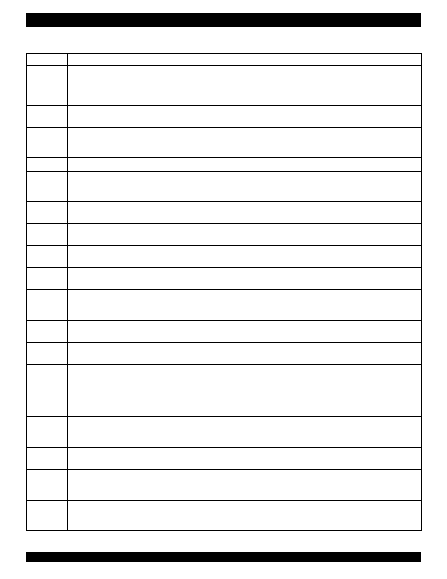
PIN DESCRIPTION
Name
Type
Pin Number
Description
GNDA1
GNDA2
GNDA3
GNDA4
Ground
50
54
59
63
Analog Ground.
All ground pins should be connected together.
GNDD
Ground
21
Digital Ground.
All digital signals are referred to this pin.
VDDA12
VDDA34
Power
52
61
+5 V Analog Power Supply.
These pins should be connected to ground via a 0.1 F capacitor. All power supply pins should be
connected together.
VDDD
Power
24
+5 V Digital Power Supply.
VDDB
Power
57
+5 V Analog Power Supply.
This pin should be connected to ground via a 0.1 F capacitor. All power supply pins should be connected
together.
CNF
56
Capacitor Noise Filter.
This pin should be connected to ground via a 0.22 F capacitor.
VIN1-4
I
49, 55, 58, 64
Analog Voice Inputs of Channel 1-4.
These pins should be connected to the corresponding SLIC via a 0.22 F capacitor.
VOUT1-4
O
51, 53, 60, 62
Voice Frequency Receiver Outputs of Channel 1-4.
These pins can drive 300
AC load. It can drive transformers directly.
SI1_(1-4)
SI2_(1-4)
I
36, 47, 2, 13
35, 48, 1, 14
SLIC Signalling Inputs with debounce function for Channel 1-4.
SB1_(1-4)
SB2_(1-4)
SB3_(1-4)
I/O
39, 44, 5, 10
38, 45, 4, 11
37, 46, 3, 12
Bi-directional SLIC Signalling I/Os for Channel 1-4.
These pins can be individually programmed as input or output.
SO1_(1-4)
SO2_(1-4)
O
41, 42, 7, 8
40, 43, 6, 9
SLIC Signalling Outputs for Channel 1-4.
DX1
O26
Transmit PCM Data Output, PCM Highway One.
Transmit PCM Data to PCM highway one. This pin is a tri-state output pin.
DX2
O29
Transmit PCM Data Output, PCM Highway Two.
Transmit PCM Data to PCM highway two. This pin is a tri-state output pin.
DR1
I27
Receive PCM Data Input, PCM Highway One.
The PCM data is received from PCM highway one (DR1) or two (DR2). The receive PCM highway is
selected by local register LREG6.
DR2
I30
Receive PCM Data Input, PCM Highway Two.
The PCM data is received from PCM highway one (DR1) or two (DR2). The receive PCM highway is
selected by local register LREG6.
FS
I31
Frame Synchronization.
FS is an 8 kHz synchronization clock that identifies the beginning of the PCM frame.
BCLK
I32
Bit Clock.
This pin clocks out the PCM data to DX1 or DX2 pin and clocks in PCM data from DR1 or DR2 pin. It may
vary from 512 kHz to 8.192 MHz and should be synchronous to FS.
TSX1
TSX2
0
25
28
Transmit Output Indicator.
The TSX1 pin becomes low when PCM data is transmitted via DX1. Open-drain.
The TSX2 pin becomes low when PCM data is transmitted via DX2. Open-drain.
相关PDF资料 |
PDF描述 |
|---|---|
| MCIMX357CVM5BR2 | IC MPU I.MX35 400MAPBGA |
| MCIMX357CVM5B | IC MPU I.MX35 400MAPBGA |
| MCIMX357CJQ5CR2 | MULTIMEDIA PROCESSOR 400-MAPBGA |
| MCF5270CVM150J | IC MCU 32BIT 150MHZ 196-MAPBGA |
| ADV202BBCZ-150 | IC VIDEO CODEC JPEG2000 144CSBGA |
相关代理商/技术参数 |
参数描述 |
|---|---|
| IDT821064 | 制造商:IDT 制造商全称:Integrated Device Technology 功能描述:QUAD PROGRAMMABLE PCM CODEC WITH GCI INTERFACE |
| IDT821064PQF | 制造商:IDT 制造商全称:Integrated Device Technology 功能描述:QUAD PROGRAMMABLE PCM CODEC WITH GCI INTERFACE |
| IDT821068 | 制造商:IDT 制造商全称:Integrated Device Technology 功能描述:OCTAL PROGRAMMABLE PCM CODEC |
| IDT821068PX | 制造商:IDT 制造商全称:Integrated Device Technology 功能描述:OCTAL PROGRAMMABLE PCM CODEC |
| IDT821621 | 制造商:IDT 制造商全称:Integrated Device Technology 功能描述:LONG HAUL SLIC |
发布紧急采购,3分钟左右您将得到回复。