- 您现在的位置:买卖IC网 > PDF目录30712 > L64005-F (LSI CORP) SPECIALTY CONSUMER CIRCUIT, PQFP160 PDF资料下载
参数资料
| 型号: | L64005-F |
| 厂商: | LSI CORP |
| 元件分类: | 消费家电 |
| 英文描述: | SPECIALTY CONSUMER CIRCUIT, PQFP160 |
| 封装: | PLASTIC, QFP-160 |
| 文件页数: | 185/272页 |
| 文件大小: | 1252K |
| 代理商: | L64005-F |
第1页第2页第3页第4页第5页第6页第7页第8页第9页第10页第11页第12页第13页第14页第15页第16页第17页第18页第19页第20页第21页第22页第23页第24页第25页第26页第27页第28页第29页第30页第31页第32页第33页第34页第35页第36页第37页第38页第39页第40页第41页第42页第43页第44页第45页第46页第47页第48页第49页第50页第51页第52页第53页第54页第55页第56页第57页第58页第59页第60页第61页第62页第63页第64页第65页第66页第67页第68页第69页第70页第71页第72页第73页第74页第75页第76页第77页第78页第79页第80页第81页第82页第83页第84页第85页第86页第87页第88页第89页第90页第91页第92页第93页第94页第95页第96页第97页第98页第99页第100页第101页第102页第103页第104页第105页第106页第107页第108页第109页第110页第111页第112页第113页第114页第115页第116页第117页第118页第119页第120页第121页第122页第123页第124页第125页第126页第127页第128页第129页第130页第131页第132页第133页第134页第135页第136页第137页第138页第139页第140页第141页第142页第143页第144页第145页第146页第147页第148页第149页第150页第151页第152页第153页第154页第155页第156页第157页第158页第159页第160页第161页第162页第163页第164页第165页第166页第167页第168页第169页第170页第171页第172页第173页第174页第175页第176页第177页第178页第179页第180页第181页第182页第183页第184页当前第185页第186页第187页第188页第189页第190页第191页第192页第193页第194页第195页第196页第197页第198页第199页第200页第201页第202页第203页第204页第205页第206页第207页第208页第209页第210页第211页第212页第213页第214页第215页第216页第217页第218页第219页第220页第221页第222页第223页第224页第225页第226页第227页第228页第229页第230页第231页第232页第233页第234页第235页第236页第237页第238页第239页第240页第241页第242页第243页第244页第245页第246页第247页第248页第249页第250页第251页第252页第253页第254页第255页第256页第257页第258页第259页第260页第261页第262页第263页第264页第265页第266页第267页第268页第269页第270页第271页第272页
L64005 MPEG-2 Audio/Video Decoder Technical Manual
A-3
Final Rev F
Copyright 1996 by LSI Logic Corporation. All rights reserved.
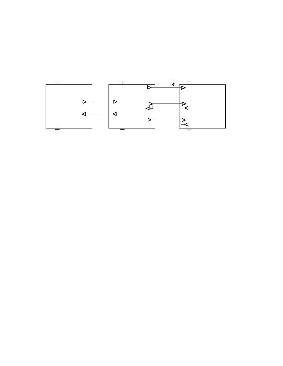
Figure A.17
5V Interface
Congurations
For each conguration, a special purpose 5-V compatible I/O buffer is
available in the technology used for L64005, which accepts signal voltage
levels exceeding the 3.3-V on-chip power supply during normal system
operation.
5-V compatible buffers are designed to interface to 5-V ICs
without being true 5-V I/Os—they do not need a 5-V power supply on-
chip.
A.2.5
5V-Compatible
Input Buffers
5-V compatible input buffers on the L64005 are designed to:
Accept valid TTL or 5-V CMOS input levels at the device pad and
guarantee proper switching
Limit voltage stress on any internal transistor to less than the maxi-
mum 3.63 V allowed across any two device terminals
Provide adequate AC performance
Exhibit acceptable levels of input leakage current in the input stage
Accept 5-V DC signals with minimal input leakage current into the
ESD protection circuitry
Withstand transient voltages similar to the maximum transient volt-
ages accepted by 5-V ICs (VIN = 6.5V)
A.2.5.1 DC Characteristics
Table A.12 shows the DC characteristics . All limits are specied over
commercial conditions. Note that absolute maximum limits for voltage
undershoot and overshoot are -1.0 V and +6.5 V.
5 V
5 V IC
L64005
3.3 V
Bidirectional
Buffer
Open
Drain
Output
5 V
R
5 V
5 V IC
3-State
Buffer
Input
Output
相关PDF资料 |
PDF描述 |
|---|---|
| L64007 | SPECIALTY CONSUMER CIRCUIT, PQFP160 |
| L64013A1 | SPECIALTY CONSUMER CIRCUIT, PQFP100 |
| L64014A | SPECIALTY CONSUMER CIRCUIT, PQFP144 |
| L64015 | SPECIALTY CONSUMER CIRCUIT, PQFP144 |
| L64020XDC | SPECIALTY CONSUMER CIRCUIT, CBGA208 |
相关代理商/技术参数 |
参数描述 |
|---|---|
| L64010ADC | 制造商:未知厂家 制造商全称:未知厂家 功能描述:Multiplier/Accumulator |
| L64010ADCC | 制造商:未知厂家 制造商全称:未知厂家 功能描述:Multiplier/Accumulator |
| L64010ADM | 制造商:未知厂家 制造商全称:未知厂家 功能描述:Multiplier/Accumulator |
| L64010ADMB | 制造商:未知厂家 制造商全称:未知厂家 功能描述:Multiplier/Accumulator |
| L64010ADMC | 制造商:未知厂家 制造商全称:未知厂家 功能描述:Multiplier/Accumulator |
发布紧急采购,3分钟左右您将得到回复。