- 您现在的位置:买卖IC网 > PDF目录385639 > MT48LC2M32LFFC (Micron Technology, Inc.) 512K x 32 x 4 banks 3.3v SDRAM(3.3V,512K x 32 x 4组同步动态RAM) PDF资料下载
参数资料
| 型号: | MT48LC2M32LFFC |
| 厂商: | Micron Technology, Inc. |
| 英文描述: | 512K x 32 x 4 banks 3.3v SDRAM(3.3V,512K x 32 x 4组同步动态RAM) |
| 中文描述: | 为512k × 32 × 4银行3.3V的内存电压(3.3V,512K采样× 32 × 4组同步动态RAM)的 |
| 文件页数: | 13/50页 |
| 文件大小: | 1054K |
| 代理商: | MT48LC2M32LFFC |
第1页第2页第3页第4页第5页第6页第7页第8页第9页第10页第11页第12页当前第13页第14页第15页第16页第17页第18页第19页第20页第21页第22页第23页第24页第25页第26页第27页第28页第29页第30页第31页第32页第33页第34页第35页第36页第37页第38页第39页第40页第41页第42页第43页第44页第45页第46页第47页第48页第49页第50页
13
64Mb: x32, 3.3V SDRAM
BatRam_3V.p65 – Rev. 0.7, Pub. 2/01
Micron Technology, Inc., reserves the right to change products or specifications without notice.
2001, Micron Technology, Inc.
64Mb: x32, 3.3V
SDRAM
PRELIMINARY
Figure 5
READ Command
Figure 6
CAS Latency
CS#
WE#
CAS#
RAS#
CKE
CLK
COLUMN
ADDRESS
A0–A7
A10
BA0, 1
HIGH
ENABLE AUTO PRECHARGE
DISABLE AUTO PRECHARGE
BANK
ADDRESS
A8, A9
CLK
DQ
T2
T1
T3
T0
CAS Latency = 3
LZ
t
D
OUT
tOH
COMMAND
NOP
READ
tAC
NOP
T4
NOP
DON’T CARE
UNDEFINED
CLK
DQ
T2
T1
T0
CAS Latency = 1
LZ
t
D
OUT
tOH
COMMAND
NOP
READ
tAC
CLK
DQ
T2
T1
T3
T0
CAS Latency = 2
LZ
t
D
OUT
tOH
COMMAND
NOP
READ
tAC
NOP
REA Ds
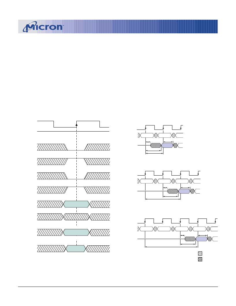
READ bursts are initiated with a READ command,
as shown in Figure 5.
The starting column and bank addresses are pro-
vided with the READ command, and auto precharge is
either enabled or disabled for that burst access. If auto
precharge is enabled, the row being accessed is
precharged at the completion of the burst. For the ge-
neric READ commands used in the following illustra-
tions, auto precharge is disabled.
During READ bursts, the valid data-out element
from the starting column address will be available fol-
lowing the CAS latency after the READ command. Each
subsequent data-out element will be valid by the next
positive clock edge. Figure 6 shows general timing for
each possible CAS latency setting.
Upon completion of a burst, assuming no other com-
mands have been initiated, the DQs will go High-Z. A
full-page burst will continue until terminated. (At the
end of the page, it will wrap to column 0 and continue.)
Data from any READ burst may be truncated with a
subsequent READ command, and data from a fixed-
length READ burst may be immediately followed by
data from a READ command. In either case, a continu-
ous flow of data can be maintained. The first data ele-
ment from the new burst follows either the last ele-
ment of a completed burst or the last desired data ele-
ment of a longer burst that is being truncated. The new
READ command should be issued
x
cycles before the
clock edge at which the last desired data element is
valid, where
x
equals the CAS latency minus one. This
is shown in Figure 7 for CAS latencies of one, two, and
相关PDF资料 |
PDF描述 |
|---|---|
| MT48LC4M16A2 | SYNCHRONOUS DRAM |
| MT48LC16M4A2 | RSD Series - Econoline Unregulated DC-DC Converters; Input Voltage (Vdc): 24V; Output Voltage (Vdc): 3.3V; Power: 1W; 1kVDC and 3kVDC Isolation Options; Approved for Medical Applications; Suitable for Automated Assembly; 8, 10 and 12 pin Pinning Style Options; Optional Continuous Short Circuit Protected; Efficiency to 85% |
| MT48LC8M16A2 | SYNCHRONOUS DRAM |
| MT48V2M32LFFC | 512K x 32 x 4 banks 2.5V SDRAM(2.5V,512K x 32 x 4组同步动态RAM) |
| MT48V4M32LFFC | SYNCHRONOUS DRAM |
相关代理商/技术参数 |
参数描述 |
|---|---|
| MT48LC2M3B2B51 | 制造商:MICRON 制造商全称:Micron Technology 功能描述:SDR SDRAM MT48LC2M32B2 a?? 512K x 32 x 4 Banks |
| MT48LC2M8A1 | 制造商:MICRON 制造商全称:Micron Technology 功能描述:SYNCHRONOUS DRAM |
| MT48LC2M8A1TGS | 制造商:MICRON 制造商全称:Micron Technology 功能描述:SYNCHRONOUS DRAM |
| MT48LC2M8A2 | 制造商:MICRON 制造商全称:Micron Technology 功能描述:SYNCHRONOUS DRAM |
| MT48LC32M16A2 | 制造商:MICRON 制造商全称:Micron Technology 功能描述:512Mb x4, x8, x16 SDRAM |
发布紧急采购,3分钟左右您将得到回复。