- 您现在的位置:买卖IC网 > PDF目录385639 > MT48LC2M32LFFC (Micron Technology, Inc.) 512K x 32 x 4 banks 3.3v SDRAM(3.3V,512K x 32 x 4组同步动态RAM) PDF资料下载
参数资料
| 型号: | MT48LC2M32LFFC |
| 厂商: | Micron Technology, Inc. |
| 英文描述: | 512K x 32 x 4 banks 3.3v SDRAM(3.3V,512K x 32 x 4组同步动态RAM) |
| 中文描述: | 为512k × 32 × 4银行3.3V的内存电压(3.3V,512K采样× 32 × 4组同步动态RAM)的 |
| 文件页数: | 20/50页 |
| 文件大小: | 1054K |
| 代理商: | MT48LC2M32LFFC |
第1页第2页第3页第4页第5页第6页第7页第8页第9页第10页第11页第12页第13页第14页第15页第16页第17页第18页第19页当前第20页第21页第22页第23页第24页第25页第26页第27页第28页第29页第30页第31页第32页第33页第34页第35页第36页第37页第38页第39页第40页第41页第42页第43页第44页第45页第46页第47页第48页第49页第50页
20
64Mb: x32, 3.3V SDRAM
BatRam_3V.p65 – Rev. 0.7, Pub. 2/01
Micron Technology, Inc., reserves the right to change products or specifications without notice.
2001, Micron Technology, Inc.
64Mb: x32, 3.3V
SDRAM
PRELIMINARY
Figure 18
WRITE To PRECHARGE
Figure 17
WRITE To READ
Figure 16
Random WRITE Cycles
CLK
DQ
D
IN
n
T2
T1
T3
T0
COMMAND
ADDRESS
WRITE
BANK,
COL
n
D
IN
a
D
IN
x
D
IN
m
WRITE
WRITE
WRITE
BANK,
COL
a
BANK,
COL
x
BANK,
COL
m
NOTE:
Each WRITE command may be to any bank.
DQM is LOW.
CLK
DQ
T2
T1
T3
T0
COMMAND
ADDRESS
NOP
WRITE
BANK,
COL
n
D
IN
n
D
IN
n
+ 1
D
OUT
b
READ
NOP
NOP
BANK,
COL
b
NOP
D
OUT
b
+ 1
T4
T5
NOTE:
The WRITE command may be to any bank, and the READ command
may be to any bank. DQM is LOW. CAS latency = 2 for illustration.
DON’T CARE
DQM
CLK
DQ
T2
T1
T4
T3
T0
COMMAND
ADDRESS
BANK
a
,
COL
n
T5
NOP
WRITE
PRECHARGE
NOP
NOP
D
IN
n
D
IN
n
+ 1
ACTIVE
tRP
BANK
(
a
or all)
t
WR
BANK
a
,
ROW
DQM
DQ
COMMAND
ADDRESS
BANK
a
,
COL
n
NOP
WRITE
PRECHARGE
NOP
NOP
D
IN
n
D
IN
n
+ 1
ACTIVE
tRP
BANK
(
a
or all)
t
WR
NOTE:
DQM could remain LOW in this example if the WRITE burst is a fixed
length of two.
BANK
a
,
ROW
T6
NOP
NOP
t
WR = 2 CLK (when
t
WR >
t
CK)
t
WR = 1 CLK (
t
CK >
t
WR)
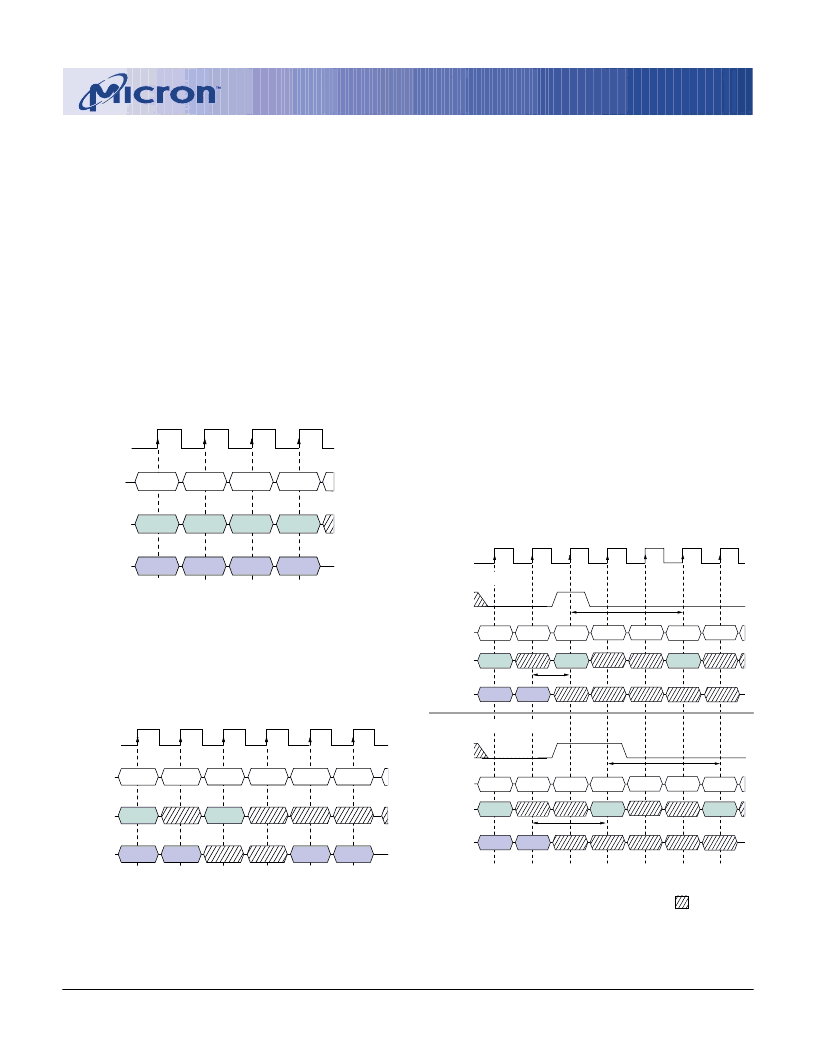
page can be performed to the same bank, as shown in
Figure 16, or each subsequent WRITE may be per-
formed to a different bank.
Data for any WRITE burst may be truncated with a
subsequent READ command, and data for a fixed-
length WRITE burst may be immediately followed by a
READ command. Once the READ command is regis-
tered, the data inputs will be ignored, and WRITEs will
not be executed. An example is shown in Figure 17.
Data
n
+ 1 is either the last of a burst of two or the last
desired of a longer burst.
Data for a fixed-length WRITE burst may be fol-
lowed by, or truncated with, a PRECHARGE command
to the same bank (provided that auto precharge was
not activated), and a full-page WRITE burst may be
truncated with a PRECHARGE command to the same
bank. The PRECHARGE command should be issued
t
WR after the clock edge at which the last desired input
data element is registered. The “two-clock” write-back
requires at least one clock plus time, regardless of fre-
quency, in auto precharge mode. In addition, when
truncating a WRITE burst, the DQM signal must be
used to mask input data for the clock edge prior to, and
the clock edge coincident with, the PRECHARGE com-
mand. An example is shown in Figure 18. Data
n
+ 1 is
either the last of a burst of two or the last desired of a
longer burst. Following the PRECHARGE command, a
subsequent command to the same bank cannot be
issued until
t
RP is met. The precharge will actually be-
gin coincident with the clock-edge (T2 in figure 18) on
an “one clock”
t
WR and sometime between the first
and second clock on an “two clock”
t
WR (between T2
and T3 in Figure 18.)
In the case of a fixed-length burst being executed to
completion, a PRECHARGE command issued at the
optimum time (as described above) provides the same
operation that would result from the same fixed-length
burst with auto precharge. The disadvantage of the
PRECHARGE command is that it requires that the com-
mand and address buses be available at the appropri-
ate time to issue the command; the advantage of the
相关PDF资料 |
PDF描述 |
|---|---|
| MT48LC4M16A2 | SYNCHRONOUS DRAM |
| MT48LC16M4A2 | RSD Series - Econoline Unregulated DC-DC Converters; Input Voltage (Vdc): 24V; Output Voltage (Vdc): 3.3V; Power: 1W; 1kVDC and 3kVDC Isolation Options; Approved for Medical Applications; Suitable for Automated Assembly; 8, 10 and 12 pin Pinning Style Options; Optional Continuous Short Circuit Protected; Efficiency to 85% |
| MT48LC8M16A2 | SYNCHRONOUS DRAM |
| MT48V2M32LFFC | 512K x 32 x 4 banks 2.5V SDRAM(2.5V,512K x 32 x 4组同步动态RAM) |
| MT48V4M32LFFC | SYNCHRONOUS DRAM |
相关代理商/技术参数 |
参数描述 |
|---|---|
| MT48LC2M3B2B51 | 制造商:MICRON 制造商全称:Micron Technology 功能描述:SDR SDRAM MT48LC2M32B2 a?? 512K x 32 x 4 Banks |
| MT48LC2M8A1 | 制造商:MICRON 制造商全称:Micron Technology 功能描述:SYNCHRONOUS DRAM |
| MT48LC2M8A1TGS | 制造商:MICRON 制造商全称:Micron Technology 功能描述:SYNCHRONOUS DRAM |
| MT48LC2M8A2 | 制造商:MICRON 制造商全称:Micron Technology 功能描述:SYNCHRONOUS DRAM |
| MT48LC32M16A2 | 制造商:MICRON 制造商全称:Micron Technology 功能描述:512Mb x4, x8, x16 SDRAM |
发布紧急采购,3分钟左右您将得到回复。