- 您现在的位置:买卖IC网 > PDF目录69040 > MT8952BPR (ZARLINK SEMICONDUCTOR INC) 1 CHANNEL(S), 2.5M bps, SERIAL COMM CONTROLLER, PQCC28 PDF资料下载
参数资料
| 型号: | MT8952BPR |
| 厂商: | ZARLINK SEMICONDUCTOR INC |
| 元件分类: | 微控制器/微处理器 |
| 英文描述: | 1 CHANNEL(S), 2.5M bps, SERIAL COMM CONTROLLER, PQCC28 |
| 封装: | PLASTIC, MS-018AB, LCC-28 |
| 文件页数: | 23/32页 |
| 文件大小: | 602K |
| 代理商: | MT8952BPR |
第1页第2页第3页第4页第5页第6页第7页第8页第9页第10页第11页第12页第13页第14页第15页第16页第17页第18页第19页第20页第21页第22页当前第23页第24页第25页第26页第27页第28页第29页第30页第31页第32页
MT8952B
Data Sheet
3
Zarlink Semiconductor Inc.
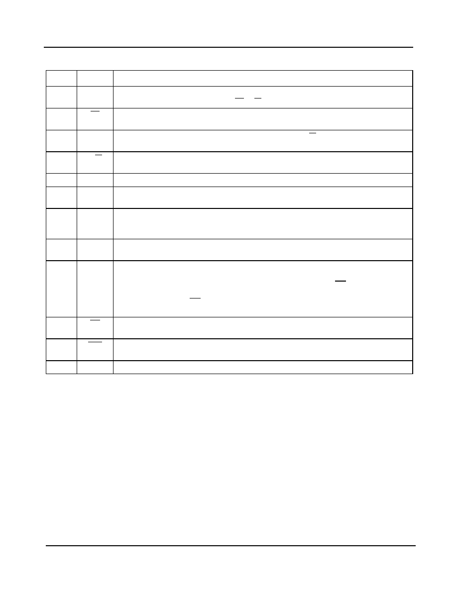
7-10
A0-A3
Address Bus Inputs - These bits address the various registers in the Protocol Controller. They select
the internal registers in conjunction with CS, R/W inputs and E Clock. (Refer to Table 1.)
11
CS
Chip Select Input - This is an active LOW input enabling the Read or Write operation to various
registers in the Protocol Controller.
12
E
Enable Clock Input - This input activates the Address Bus and R/W input and enables data transfers
on the Data Bus.
13
R/W
Read/Write Control - This input controls the direction of data flow on the data bus. When HIGH, the
I/O buffer acts as an output driver and as an input buffer when LOW.
14
VSS
Ground (0 Volt).
15-22
D0-D7
Bidirectional Data Bus - These Data Bus I/O ports allow the data transfer between the HDLC
Protocol Controller and the microprocessor.
23
REOP
Receive End Of Packet (Output) - This is a HIGH going pulse that occurs for one bit duration when
a closing flag is detected on the incoming packets, or the incoming packet is aborted, or when an
invalid packet of 24 or more bits is received.
24
TEOP
Transmit End Of Packet (Output) - This is a HIGH going pulse that occurs for one bit duration
when a packet is transmitted correctly or aborted.
25
CKi
Clock Input (Bit rate clock or 2 x bit rate clock in ST-BUS format while in the Internal Timing
Mode and bit rate Clock in the External Timing Mode) - This is the clock input used for shifting
in/out the formatted packets. It can be at bit rate (C2i) or twice the bit rate (C4i) in ST-BUS format
while the Protocol Controller is in the Internal Timing Mode. Whether the clock should be C2i
(typically 2.048 MHz) or C4i (typically 4.096 MHz) is decided by the BRCK bit in the Timing
Control Register. If the Protocol Controller is in the External Timing Mode, it is at the bit rate.
26
F0i
Frame Pulse Input - This is the frame pulse input in ST-BUS format to establish the beginning of the
frame in the Internal Timing Mode. This is also the signal clocking the watchdog timer.
27
RST
RESET Input - This is an active LOW Schmitt Trigger input, resetting all the registers including the
transmit and receive FIFOs and the watchdog timer.
28
VDD
Supply (5 Volts).
Pin Description (continued)
Pin No.
Name
Description
相关PDF资料 |
PDF描述 |
|---|---|
| MT8952BP1 | 1 CHANNEL(S), 2.5M bps, SERIAL COMM CONTROLLER, PQCC28 |
| MTA41110/P | SPECIALTY MICROPROCESSOR CIRCUIT, PDIP18 |
| MTA41110/SO | SPECIALTY MICROPROCESSOR CIRCUIT, PDSO18 |
| MTR80C186-12 | 16-BIT, 12.5 MHz, MICROPROCESSOR, CQCC68 |
| MTA80C186-10 | 16-BIT, 10 MHz, MICROPROCESSOR, CPGA68 |
相关代理商/技术参数 |
参数描述 |
|---|---|
| MT8952BPR1 | 制造商:Microsemi Corporation 功能描述:PB FREE HDLC CONTROLLER, PLCC - Tape and Reel 制造商:Zarlink Semiconductor Inc 功能描述:PB FREE HDLC CONTROLLER, PLCC - Tape and Reel |
| MT8952BS | 制造商:Microsemi Corporation 功能描述: |
| MT8952BS1 | 制造商:Microsemi Corporation 功能描述:PB FREE HDLC PROTOCOL CONTROLLER - Rail/Tube 制造商:Zarlink Semiconductor Inc 功能描述:PB FREE HDLC PROTOCOL CONTROLLER |
| MT8960 | 制造商:ZARLINK 制造商全称:Zarlink Semiconductor Inc 功能描述:Integrated PCM Filter Codec |
| MT8960AE | 制造商:ZARLINK 功能描述: |
发布紧急采购,3分钟左右您将得到回复。