- 您现在的位置:买卖IC网 > PDF目录69040 > MT8952BPR (ZARLINK SEMICONDUCTOR INC) 1 CHANNEL(S), 2.5M bps, SERIAL COMM CONTROLLER, PQCC28 PDF资料下载
参数资料
| 型号: | MT8952BPR |
| 厂商: | ZARLINK SEMICONDUCTOR INC |
| 元件分类: | 微控制器/微处理器 |
| 英文描述: | 1 CHANNEL(S), 2.5M bps, SERIAL COMM CONTROLLER, PQCC28 |
| 封装: | PLASTIC, MS-018AB, LCC-28 |
| 文件页数: | 31/32页 |
| 文件大小: | 602K |
| 代理商: | MT8952BPR |
第1页第2页第3页第4页第5页第6页第7页第8页第9页第10页第11页第12页第13页第14页第15页第16页第17页第18页第19页第20页第21页第22页第23页第24页第25页第26页第27页第28页第29页第30页当前第31页第32页
MT8952B
Data Sheet
8
Zarlink Semiconductor Inc.
Watchdog Timer
This is a fixed eleven stage binary counter with F0i as the input and WD as the output from the last stage. This
counter can be reset either by the external input (RST) or by writing XXX0 1010 to the Watchdog Timer Register.
The WD output is normally HIGH and if the Watchdog Timer Register is not written within 210 cycles of F0i input
after it is reset, the WD output will go LOW for a period of 210 cycles of F0i.
Even though the F0i input is not
required for formatting data in the External Timing Mode, it is necessary for the operation of the watchdog timer.
Order of Bit Transmission/Reception
The Least Significant Bit (LSB) corresponding to D0 on the data bus is transmitted first on the serial output
(CDSTo). On the receiving side, the first bit received on the serial input (CDSTi) is considered as the LSB and
placed on D0 of the data bus.
Registers
There are several registers in the HDLC Protocol Controller accessible to the associated micro-processor via the
data bus. The addresses of these registers are given in Table 1 and their functional details are given below.
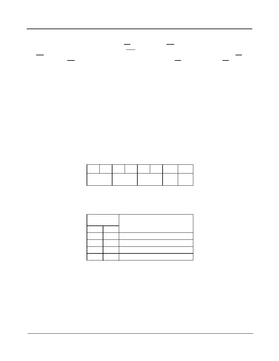
FIFO Status Register (Read)
This register (Figure 4) indicates the status of transmit and receive FIFOs and the received byte as described
below.
Figure 4 - FIFO Status Register
Rx Byte Status: These two bits (D7 and D6) indicate the status of the received byte ready to be read from the
receive FIFO. The status is encoded as shown in Table 3.
Table 3 - Received Byte Status
Rx FIFO Status: These bits (D5 and D4) indicate the status of receive FIFO as given by Table 4. The Rx FIFO
status bits are not updated immediately after an access of the Rx FIFO (a read from the microprocessor port, or a
write from the serial port), to avoid the existence of unrecoverable error conditions.
When in external timing mode, the MT8952B must receive two falling edges of the clock signal at the CKi input
before the Rx FIFO status bits will be updated. When in internal 2.048 MHz timing mode, the MT8952B must
receive two falling edges of the C2i clock before the Rx FIFO status bits will be updated. When in internal 4.096 MHz
timing mode, the MT8952B must receive four falling edges of the C4i clock before the Rx FIFO status bit will be updated
(see the section on Receive Operation - Normal Packets).
D7
D6
D5
D4
D3
D2
D1
D0
Rx Byte
Status
Rx FIFO
Status
Tx FIFO
Status
LOW
Rx Byte
Status Bits
Status
D7
D6
0
Packet Byte
0
1
First Byte
1
0
Last Byte (Good FCS)
1
Last Byte (Bad FCS)
相关PDF资料 |
PDF描述 |
|---|---|
| MT8952BP1 | 1 CHANNEL(S), 2.5M bps, SERIAL COMM CONTROLLER, PQCC28 |
| MTA41110/P | SPECIALTY MICROPROCESSOR CIRCUIT, PDIP18 |
| MTA41110/SO | SPECIALTY MICROPROCESSOR CIRCUIT, PDSO18 |
| MTR80C186-12 | 16-BIT, 12.5 MHz, MICROPROCESSOR, CQCC68 |
| MTA80C186-10 | 16-BIT, 10 MHz, MICROPROCESSOR, CPGA68 |
相关代理商/技术参数 |
参数描述 |
|---|---|
| MT8952BPR1 | 制造商:Microsemi Corporation 功能描述:PB FREE HDLC CONTROLLER, PLCC - Tape and Reel 制造商:Zarlink Semiconductor Inc 功能描述:PB FREE HDLC CONTROLLER, PLCC - Tape and Reel |
| MT8952BS | 制造商:Microsemi Corporation 功能描述: |
| MT8952BS1 | 制造商:Microsemi Corporation 功能描述:PB FREE HDLC PROTOCOL CONTROLLER - Rail/Tube 制造商:Zarlink Semiconductor Inc 功能描述:PB FREE HDLC PROTOCOL CONTROLLER |
| MT8960 | 制造商:ZARLINK 制造商全称:Zarlink Semiconductor Inc 功能描述:Integrated PCM Filter Codec |
| MT8960AE | 制造商:ZARLINK 功能描述: |
发布紧急采购,3分钟左右您将得到回复。