- 您现在的位置:买卖IC网 > PDF目录369948 > PC28F256J3C-115 (Intel Corp.) Intel StrataFlash Memory (J3) PDF资料下载
参数资料
| 型号: | PC28F256J3C-115 |
| 厂商: | Intel Corp. |
| 英文描述: | Intel StrataFlash Memory (J3) |
| 中文描述: | 英特尔StrataFlash存储器(J3) |
| 文件页数: | 32/72页 |
| 文件大小: | 905K |
| 代理商: | PC28F256J3C-115 |
第1页第2页第3页第4页第5页第6页第7页第8页第9页第10页第11页第12页第13页第14页第15页第16页第17页第18页第19页第20页第21页第22页第23页第24页第25页第26页第27页第28页第29页第30页第31页当前第32页第33页第34页第35页第36页第37页第38页第39页第40页第41页第42页第43页第44页第45页第46页第47页第48页第49页第50页第51页第52页第53页第54页第55页第56页第57页第58页第59页第60页第61页第62页第63页第64页第65页第66页第67页第68页第69页第70页第71页第72页
256-Mbit J3 (x8/x16)
32
Datasheet
9.0
Bus Operations
This section provides an overview of device bus operations. The on-chip Write State Machine
(WSM) manages all erase and program algorithms. The system CPU provides control of all in-
system read, write, and erase operations of the device via the system bus.
Device commands are written to the CUI to control all of the flash memory device’s operations.
The CUI does not occupy an addressable memory location; it’s the mechanism through which the
flash device is controlled.
9.1
Bus Operations Overview
The local CPU reads and writes flash memory in-system. All bus cycles to or from the flash
memory conform to standard microprocessor bus cycles.
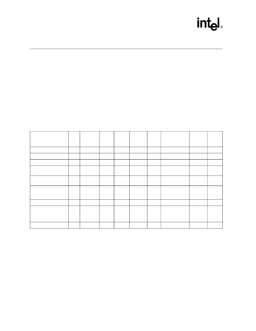
Table 12. Bus Operations
Mode
RP#
CE[2:0]
(1)
OE#
(2)
WE#
(2)
Address
VPEN
Data
(3)
STS
(default
mode)
Notes
Read Array
V
IH
V
IH
Enabled
V
IL
V
IH
V
IH
V
IH
X
X
D
OUT
High Z
High Z
(7)
4,5,6
Output Disable
Enabled
X
X
X
Standby
V
IH
Disabled
X
X
X
X
High Z
X
Reset/Power-Down
Mode
V
IL
X
X
X
X
X
High Z
High Z
(7)
Read Identifier Codes
V
IH
Enabled
V
IL
V
IH
See
Table 17
X
Note 8
High Z
(7)
Read Query
V
IH
Enabled
V
IL
V
IH
See
Table
10.3
X
Note 9
High Z
(7)
Read Status (WSM off)
V
IH
Enabled
V
IL
V
IH
X
X
D
OUT
D7
= D
OUT
D[15:8]
= High Z
D[6:0]
= High Z
Read Status (WSM on)
V
IH
Enabled
V
IL
V
IH
X
X
Write
V
IH
Enabled
V
IH
V
IL
X
V
PENH
D
IN
X
6,10,11
NOTES:
1. See
Table 13 on page 33
for valid CE configurations.
2. OE# and WE# should never be enabled simultaneously.
3. D refers to D[7:0] if BYTE# is low and D[15:0] if BYTE# is high.
4. Refer to
DC Characteristics
. When V
≤
V
, memory contents can be read, but not altered.
5. X can be V
or V
IH
for control and address signals, and V
PENLK
or V
PENH
for V
PEN
. See
DC Characteristics
for V
PENLK
and
V
voltages.
6. In default mode, STS is V
when the WSM is executing internal block erase, program, or lock-bit configuration algorithms. It
is V
when the WSM is not busy, in block erase suspend mode (with programming inactive), program suspend mode, or
reset/power-down mode.
7. High Z will be V
with an external pull-up resistor.
8. See
Section 10.2, “Read Identifier Codes” on page 39
for read identifier code data.
9. See
Section 10.3, “Read Query/CFI” on page 41
for read query data.
10.Command writes involving block erase, program, or lock-bit configuration are reliably executed when V
PEN
= V
PENH
and V
CC
is within specification.
相关PDF资料 |
PDF描述 |
|---|---|
| PC28F128J3C-115 | Intel StrataFlash Memory (J3) |
| PC28F640J3C-115 | Intel StrataFlash Memory (J3) |
| PC28F320J3C-115 | Intel StrataFlash Memory (J3) |
| PC28F128J3C-120 | Intel StrataFlash Memory (J3) |
| PC28F128J3C-125 | Intel StrataFlash Memory (J3) |
相关代理商/技术参数 |
参数描述 |
|---|---|
| PC28F256J3C-120 | 制造商:INTEL 制造商全称:Intel Corporation 功能描述:Intel StrataFlash Memory (J3) |
| PC28F256J3C125 | 制造商:INTEL 制造商全称:Intel Corporation 功能描述:Intel StrataFlash?? Memory |
| PC28F256J3C-125 | 制造商:INTEL 制造商全称:Intel Corporation 功能描述:Intel StrataFlash Memory (J3) |
| PC28F256J3C125 S B93 | 制造商:Intel 功能描述: |
| PC28F256J3C-150 | 制造商:INTEL 制造商全称:Intel Corporation 功能描述:Intel StrataFlash Memory (J3) |
发布紧急采购,3分钟左右您将得到回复。