- 您现在的位置:买卖IC网 > PDF目录369948 > PC28F256J3C-115 (Intel Corp.) Intel StrataFlash Memory (J3) PDF资料下载
参数资料
| 型号: | PC28F256J3C-115 |
| 厂商: | Intel Corp. |
| 英文描述: | Intel StrataFlash Memory (J3) |
| 中文描述: | 英特尔StrataFlash存储器(J3) |
| 文件页数: | 39/72页 |
| 文件大小: | 905K |
| 代理商: | PC28F256J3C-115 |
第1页第2页第3页第4页第5页第6页第7页第8页第9页第10页第11页第12页第13页第14页第15页第16页第17页第18页第19页第20页第21页第22页第23页第24页第25页第26页第27页第28页第29页第30页第31页第32页第33页第34页第35页第36页第37页第38页当前第39页第40页第41页第42页第43页第44页第45页第46页第47页第48页第49页第50页第51页第52页第53页第54页第55页第56页第57页第58页第59页第60页第61页第62页第63页第64页第65页第66页第67页第68页第69页第70页第71页第72页
256-Mbit J3 (x8/x16)
Datasheet
39
10.2
Read Identifier Codes
The Read identifier codes operation outputs the manufacturer code, device-code, and the block
lock configuration codes for each block (See
Section 9.2, “Device Commands” on page 35
for
details on issuing the Read Device Identifier command). Page-mode reads are not supported in this
read mode. To terminate the operation, write another valid command. Like the Read Array
command, the Read Identifier Codes command functions independently of the V
PEN
voltage. This
command is valid only when the WSM is off or the device is suspended. Following the Read
Identifier Codes command, the following information can be read.
10.2.1
Read Status Register
The Status Register may be read to determine when a block erase, program, or lock-bit
configuration is complete and whether the operation completed successfully. It may be read only
after the specified time W12 (see
Table 9, “Write Operations” on page 26
). After writing this
command, all subsequent read operations output data from the Status Register until another valid
command is written. Page-mode reads are not supported in this read mode. The Status Register
contents are latched on the falling edge of OE# or the first edge of CE0, CE1, or CE2 that enables
the device (see
Table 13, “Chip Enable Truth Table” on page 33
). OE# must toggle to V
IH
or the
device must be disabled before further reads to update the Status Register latch. The Read Status
Register command functions independently of the V
PEN
voltage.
During a program, block erase, set lock-bit, or clear lock-bit command sequence, only SR.7 is valid
until the Write State Machine completes or suspends the operation. Device I/O signals D[6:0] and
D[15:8] are placed in a high-impedance state. When the operation completes or suspends (check
SR.7), all contents of the Status Register are valid when read.
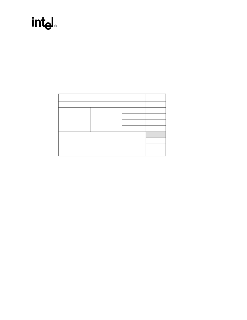
Table 17. Read Identifier Codes
Code
Address
(1)
Data
Manufacture Code
00000
(00) 89
Device Code
32-Mbit
00001
(00) 16
64-Mbit
00001
(00) 17
128-Mbit
00001
(00) 18
256-Mbit
00001
(00) 1D
Block Lock Configuration
X
0002
(2)
Block Is Unlocked
D0 = 0
Block Is Locked
D0 = 1
Reserved for Future Use
D[7:1]
NOTES:
1. A0 is not used in either x8 or x16 modes when obtaining the identifier
codes. The lowest order address line is A1. Data is always presented
on the low byte in x16 mode (upper byte contains 00h).
2. X selects the specific block’s lock configuration code.
3. D[7:1] are invalid and should be ignored.
相关PDF资料 |
PDF描述 |
|---|---|
| PC28F128J3C-115 | Intel StrataFlash Memory (J3) |
| PC28F640J3C-115 | Intel StrataFlash Memory (J3) |
| PC28F320J3C-115 | Intel StrataFlash Memory (J3) |
| PC28F128J3C-120 | Intel StrataFlash Memory (J3) |
| PC28F128J3C-125 | Intel StrataFlash Memory (J3) |
相关代理商/技术参数 |
参数描述 |
|---|---|
| PC28F256J3C-120 | 制造商:INTEL 制造商全称:Intel Corporation 功能描述:Intel StrataFlash Memory (J3) |
| PC28F256J3C125 | 制造商:INTEL 制造商全称:Intel Corporation 功能描述:Intel StrataFlash?? Memory |
| PC28F256J3C-125 | 制造商:INTEL 制造商全称:Intel Corporation 功能描述:Intel StrataFlash Memory (J3) |
| PC28F256J3C125 S B93 | 制造商:Intel 功能描述: |
| PC28F256J3C-150 | 制造商:INTEL 制造商全称:Intel Corporation 功能描述:Intel StrataFlash Memory (J3) |
发布紧急采购,3分钟左右您将得到回复。