- 您现在的位置:买卖IC网 > PDF目录378049 > PEB20550 (INFINEON TECHNOLOGIES AG) ICs for Communications PDF资料下载
参数资料
| 型号: | PEB20550 |
| 厂商: | INFINEON TECHNOLOGIES AG |
| 英文描述: | ICs for Communications |
| 中文描述: | 通信集成电路 |
| 文件页数: | 153/407页 |
| 文件大小: | 1964K |
| 代理商: | PEB20550 |
第1页第2页第3页第4页第5页第6页第7页第8页第9页第10页第11页第12页第13页第14页第15页第16页第17页第18页第19页第20页第21页第22页第23页第24页第25页第26页第27页第28页第29页第30页第31页第32页第33页第34页第35页第36页第37页第38页第39页第40页第41页第42页第43页第44页第45页第46页第47页第48页第49页第50页第51页第52页第53页第54页第55页第56页第57页第58页第59页第60页第61页第62页第63页第64页第65页第66页第67页第68页第69页第70页第71页第72页第73页第74页第75页第76页第77页第78页第79页第80页第81页第82页第83页第84页第85页第86页第87页第88页第89页第90页第91页第92页第93页第94页第95页第96页第97页第98页第99页第100页第101页第102页第103页第104页第105页第106页第107页第108页第109页第110页第111页第112页第113页第114页第115页第116页第117页第118页第119页第120页第121页第122页第123页第124页第125页第126页第127页第128页第129页第130页第131页第132页第133页第134页第135页第136页第137页第138页第139页第140页第141页第142页第143页第144页第145页第146页第147页第148页第149页第150页第151页第152页当前第153页第154页第155页第156页第157页第158页第159页第160页第161页第162页第163页第164页第165页第166页第167页第168页第169页第170页第171页第172页第173页第174页第175页第176页第177页第178页第179页第180页第181页第182页第183页第184页第185页第186页第187页第188页第189页第190页第191页第192页第193页第194页第195页第196页第197页第198页第199页第200页第201页第202页第203页第204页第205页第206页第207页第208页第209页第210页第211页第212页第213页第214页第215页第216页第217页第218页第219页第220页第221页第222页第223页第224页第225页第226页第227页第228页第229页第230页第231页第232页第233页第234页第235页第236页第237页第238页第239页第240页第241页第242页第243页第244页第245页第246页第247页第248页第249页第250页第251页第252页第253页第254页第255页第256页第257页第258页第259页第260页第261页第262页第263页第264页第265页第266页第267页第268页第269页第270页第271页第272页第273页第274页第275页第276页第277页第278页第279页第280页第281页第282页第283页第284页第285页第286页第287页第288页第289页第290页第291页第292页第293页第294页第295页第296页第297页第298页第299页第300页第301页第302页第303页第304页第305页第306页第307页第308页第309页第310页第311页第312页第313页第314页第315页第316页第317页第318页第319页第320页第321页第322页第323页第324页第325页第326页第327页第328页第329页第330页第331页第332页第333页第334页第335页第336页第337页第338页第339页第340页第341页第342页第343页第344页第345页第346页第347页第348页第349页第350页第351页第352页第353页第354页第355页第356页第357页第358页第359页第360页第361页第362页第363页第364页第365页第366页第367页第368页第369页第370页第371页第372页第373页第374页第375页第376页第377页第378页第379页第380页第381页第382页第383页第384页第385页第386页第387页第388页第389页第390页第391页第392页第393页第394页第395页第396页第397页第398页第399页第400页第401页第402页第403页第404页第405页第406页第407页
PEB 20550
PEF 20550
Detailed Register Description
Semiconductor Group
153
01.96
4.6.24
Access in demultiplexed
μ
P-interface mode:
Access in multiplexed
μ
P-interface mode:
Reset value: xx
H
MF-Channel Subscriber Address Register (MFSAR)
read/write
read/write
address: 0A
H
address: 14
H
The exchange of monitor data normally takes place with only one subscriber circuit at a
time. This register serves to point the MF-handler to that particular CFI time slot.
MFTC1..0
MF Channel Transfer Control 1..0; these bits, in addition to CMDR:MFT1,0
and OMDR:MFPS control the MF-channel transfer as indicated in
table 21
.
SAD5..0
Subscriber address 5..0; these bits define the addressed subscriber. The
CFI time slot encoding is similar to the one used for Control Memory
accesses using the MAAR-register (
tables 19
and
20
):
CFI time slot encoding of MFSAR derived from MAAR:
MAAR:MA7 selects between upstream and downstream CM-blocks. This information is
not required since the transfer direction is defined by CMDR (transmit or receive).
MAAR:MA0 selects between even and odd time slots. This information is also not
required since MF-channels are always located on even time slots.
4.6.25
Access in demultiplexed
μ
P-interface mode:
Access in multiplexed
μ
P-interface mode:
Reset value: empty
Monitor/Feature Control Channel FIFO (MFFIFO)
read/write
read/write
address: 0B
H
address: 16
H
The 16-byte bi-directional MFFIFO provides intermediate storage for data bytes to be
transmitted or received over the monitor or feature control channel.
MFD7..0
MF Data bits 7..0; MFD7 (MSB) is the first bit to be sent over the serial CFI,
MFD0 (LSB) the last.
Note: The byte n + 1 of an n-byte transmit message in monitor channel is not defined.
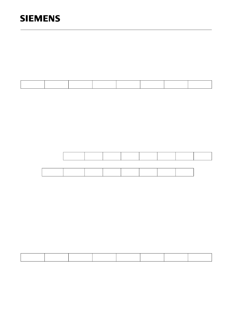
bit 7
MFTC1
bit 0
SAD0
MFTC0
SAD5
SAD4
SAD3
SAD2
SAD1
MAAR:
MA7
MA6
↓
SAD5
MA5
↓
SAD4
MA4
↓
SAD3
MA3
↓
SAD2
MA2
↓
SAD1
MA1
↓
SAD0
MA0
MFSAR: MFTC1
MFTC0
bit 7
MFD7
bit 0
MFD0
MFD6
MFD5
MFD4
MFD3
MFD2
MFD1
相关PDF资料 |
PDF描述 |
|---|---|
| PEF20570 | DSP Embedded Line and Port Interface Controller |
| PEF20571 | DSP Embedded Line and Port Interface Controller |
| PEF2080 | S/T Bus Interface Circuit(SBC) |
| PEF22554 | Ultraframer DS3/E3/DS2/E2/DS1/E1/DS0 |
| PEF22554E | Ultraframer DS3/E3/DS2/E2/DS1/E1/DS0 |
相关代理商/技术参数 |
参数描述 |
|---|---|
| PEB20550HV1.3 | 制造商:Rochester Electronics LLC 功能描述:- Bulk |
| PEB20550H-V1.3 | 制造商:Infineon Technologies AG 功能描述: |
| PEB2055-C | 制造商:未知厂家 制造商全称:未知厂家 功能描述:PCM, Other/Special/Miscellaneous |
| PEB2055K | 制造商:未知厂家 制造商全称:未知厂家 功能描述: |
| PEB2055-N | 制造商:未知厂家 制造商全称:未知厂家 功能描述:PCM, Other/Special/Miscellaneous |
发布紧急采购,3分钟左右您将得到回复。