- 您现在的位置:买卖IC网 > PDF目录69321 > RFPIC12F675K-E/SS 8-BIT, FLASH, 20 MHz, RISC MICROCONTROLLER, PDSO20 PDF资料下载
参数资料
| 型号: | RFPIC12F675K-E/SS |
| 元件分类: | 微控制器/微处理器 |
| 英文描述: | 8-BIT, FLASH, 20 MHz, RISC MICROCONTROLLER, PDSO20 |
| 封装: | 0.209 INCH, PLASTIC, MO-150, SSOP-20 |
| 文件页数: | 35/123页 |
| 文件大小: | 5438K |
| 代理商: | RFPIC12F675K-E/SS |
第1页第2页第3页第4页第5页第6页第7页第8页第9页第10页第11页第12页第13页第14页第15页第16页第17页第18页第19页第20页第21页第22页第23页第24页第25页第26页第27页第28页第29页第30页第31页第32页第33页第34页当前第35页第36页第37页第38页第39页第40页第41页第42页第43页第44页第45页第46页第47页第48页第49页第50页第51页第52页第53页第54页第55页第56页第57页第58页第59页第60页第61页第62页第63页第64页第65页第66页第67页第68页第69页第70页第71页第72页第73页第74页第75页第76页第77页第78页第79页第80页第81页第82页第83页第84页第85页第86页第87页第88页第89页第90页第91页第92页第93页第94页第95页第96页第97页第98页第99页第100页第101页第102页第103页第104页第105页第106页第107页第108页第109页第110页第111页第112页第113页第114页第115页第116页第117页第118页第119页第120页第121页第122页第123页
2003 Microchip Technology Inc.
Preliminary
DS70091A-page 17
rfPIC12F675
3.0
GPIO PORT
There are as many as six general purpose I/O pins
available.
Depending
on
which
peripherals
are
enabled, some or all of the pins may not be available as
general purpose I/O. In general, when a peripheral is
enabled, the associated pin may not be used as a
general purpose I/O pin.
3.1
GPIO and the TRISIO Registers
GPIO is an 6-bit wide, bi-directional port. The
corresponding data direction register is TRISIO.
Setting a TRISIO bit (= 1) will make the corresponding
GPIO pin an input (i.e., put the corresponding output
driver in a Hi-impedance mode). Clearing a TRISIO bit
(= 0) will make the corresponding GPIO pin an output
(i.e., put the contents of the output latch on the selected
pin). The exception is GP3, which is input only and its
TRISIO bit will always read as ‘1’. Example 3-1 shows
how to initialize GPIO.
Reading the GPIO register reads the status of the pins,
whereas writing to it will write to the port latch. All write
operations are read-modify-write operations. There-
fore, a write to a port implies that the port pins are read,
this value is modified, and then written to the port data
latch. GP3 reads ‘0’ when MCLREN = 1.
The TRISIO register controls the direction of the
GP pins, even when they are being used as analog
inputs. The user must ensure the bits in the TRISIO
register are maintained set when using them as analog
inputs. I/O pins configured as analog inputs always
read ‘0’.
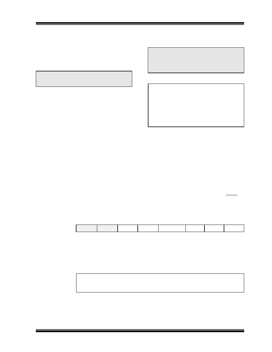
EXAMPLE 3-1:
INITIALIZING GPIO
3.2
Additional Pin Functions
Every GPIO pin on the rfPIC12F675 has an interrupt-
on-change option and every GPIO pin, except GP3,
has a weak pull-up option. The next two sections
describe these functions.
3.2.1
WEAK PULL-UP
Each of the GPIO pins, except GP3, has an individually
configurable weak internal pull-up. Control bits WPUx
enable or disable each pull-up. Refer to Register 3-3.
Each weak pull-up is automatically turned off when the
port pin is configured as an output. The pull-ups are
disabled on a Power-on Reset by the GPPU bit
(OPTION<7>).
REGISTER 3-1:
GPIO — GPIO REGISTER (ADDRESS: 05h)
Note:
Additional information on I/O ports may be
found in the PICmicro Mid-Range Refer-
ence Manual (DS33023)
Note:
The ANSEL (9Fh) and CMCON (19h)
registers (9Fh) must be initialized to
configure an analog channel as a digital
input. Pins configured as analog inputs will
read ‘0’.
bcf
STATUS,RP0
;Bank 0
clrf
GPIO
;Init GPIO
movlw
07h
;Set GP<2:0> to
movwf
CMCON
;digital IO
bsf
STATUS,RP0
;Bank 1
clrf
ANSEL
;Digital I/O
movlw
0Ch
;Set GP<3:2> as inputs
movwf
TRISIO
;and set GP<5:4,1:0>
;as outputs
U-0
R/W-x
—
GPIO5
GPIO4
GPIO3
GPIO2
GPIO1
GPIO0
bit 7
bit 0
bit 7-6:
Unimplemented: Read as ’0’
bit 5-0:
GPIO<5:0>: General Purpose I/O pin.
1 = Port pin is >VIH
0 = Port pin is <VIL
Legend:
R = Readable bit
W = Writable bit
U = Unimplemented bit, read as ‘0’
- n = Value at POR
’1’ = Bit is set
’0’ = Bit is cleared
x = Bit is unknown
相关PDF资料 |
PDF描述 |
|---|---|
| RFPIC12F675H-E/SS | 8-BIT, FLASH, 20 MHz, RISC MICROCONTROLLER, PDSO20 |
| RH80530GZ001512 | 32-BIT, 1000 MHz, MICROPROCESSOR, CPGA478 |
| RH80530GZ009512 | 32-BIT, 1200 MHz, MICROPROCESSOR, CPGA478 |
| RJ80530GZ004512 | 32-BIT, 1066 MHz, MICROPROCESSOR, PBGA479 |
| RH80530GZ004512 | 32-BIT, 1066 MHz, MICROPROCESSOR, CPGA478 |
相关代理商/技术参数 |
参数描述 |
|---|---|
| RFPIC12F675K-I/SS | 功能描述:射频微控制器 - MCU 290-350MHz UHF ASK/FSK Transmitter RoHS:否 制造商:Silicon Labs 核心:8051 处理器系列:Si100x 数据总线宽度:8 bit 最大时钟频率:24 MHz 程序存储器大小:64 KB 数据 RAM 大小:4 KB 片上 ADC:Yes 工作电源电压:1.8 V to 3.6 V 工作温度范围:- 40 C to + 85 C 封装 / 箱体:LGA-42 安装风格:SMD/SMT 封装:Tube |
| RFPIC12F675KT-I/SS | 功能描述:射频微控制器 - MCU 1 KB Flash FSK ASK RoHS:否 制造商:Silicon Labs 核心:8051 处理器系列:Si100x 数据总线宽度:8 bit 最大时钟频率:24 MHz 程序存储器大小:64 KB 数据 RAM 大小:4 KB 片上 ADC:Yes 工作电源电压:1.8 V to 3.6 V 工作温度范围:- 40 C to + 85 C 封装 / 箱体:LGA-42 安装风格:SMD/SMT 封装:Tube |
| RFPMV00 | 制造商:Carlo Gavazzi 功能描述:RSBT ALARM RELAY OUTPUT MODULE |
| RF-PP12/23 | 制造商:Cembre 功能描述:F-CRIMP,BLADE,RED,PP12/23 |
| RFP-QD10 | 功能描述:烙铁 Cartridge Quad PLCC-52 Chip Pkg RoHS:否 制造商:Weller 产品:Soldering Stations 类型:Digital, Iron, Stand, Cleaner 瓦特:50 W 最大温度:+ 850 F 电缆类型:US Cord Included |
发布紧急采购,3分钟左右您将得到回复。