- 您现在的位置:买卖IC网 > PDF目录69321 > RFPIC12F675K-E/SS 8-BIT, FLASH, 20 MHz, RISC MICROCONTROLLER, PDSO20 PDF资料下载
参数资料
| 型号: | RFPIC12F675K-E/SS |
| 元件分类: | 微控制器/微处理器 |
| 英文描述: | 8-BIT, FLASH, 20 MHz, RISC MICROCONTROLLER, PDSO20 |
| 封装: | 0.209 INCH, PLASTIC, MO-150, SSOP-20 |
| 文件页数: | 90/123页 |
| 文件大小: | 5438K |
| 代理商: | RFPIC12F675K-E/SS |
第1页第2页第3页第4页第5页第6页第7页第8页第9页第10页第11页第12页第13页第14页第15页第16页第17页第18页第19页第20页第21页第22页第23页第24页第25页第26页第27页第28页第29页第30页第31页第32页第33页第34页第35页第36页第37页第38页第39页第40页第41页第42页第43页第44页第45页第46页第47页第48页第49页第50页第51页第52页第53页第54页第55页第56页第57页第58页第59页第60页第61页第62页第63页第64页第65页第66页第67页第68页第69页第70页第71页第72页第73页第74页第75页第76页第77页第78页第79页第80页第81页第82页第83页第84页第85页第86页第87页第88页第89页当前第90页第91页第92页第93页第94页第95页第96页第97页第98页第99页第100页第101页第102页第103页第104页第105页第106页第107页第108页第109页第110页第111页第112页第113页第114页第115页第116页第117页第118页第119页第120页第121页第122页第123页
2003 Microchip Technology Inc.
Preliminary
DS70091A-page 67
rfPIC12F675
10.4.1
GP2/INT INTERRUPT
External interrupt on GP2/INT pin is edge-triggered;
either rising if INTEDG bit (OPTION<6>) is set, of
falling, if INTEDG bit is clear. When a valid edge
appears
on
the
GP2/INT
pin,
the
INTF
bit
(INTCON<1>) is set. This interrupt can be disabled by
clearing the INTE control bit (INTCON<4>). The INTF
bit must be cleared in software in the Interrupt Service
Routine before re-enabling this interrupt. The GP2/INT
interrupt can wake-up the processor from SLEEP if the
INTE bit was set prior to going into SLEEP. The status
of the GIE bit decides whether or not the processor
branches to the interrupt vector following wake-up. See
Section 10.9 for details on SLEEP and Figure 10-13 for
timing of wake-up from SLEEP through GP2/INT
interrupt.
10.4.2
TMR0 INTERRUPT
An overflow (FFh
→ 00h) in the TMR0 register will
set the T0IF (INTCON<2>) bit. The interrupt can
be
enabled/disabled
by
setting/clearing
T0IE
(INTCON<5>) bit. For operation of the Timer0 module,
see Section 4.0.
10.4.3
GPIO INTERRUPT
An input change on GPIO change sets the GPIF
(INTCON<0>) bit. The interrupt can be enabled/
disabled by setting/clearing the GPIE (INTCON<3>)
bit. Plus individual pins can be configured through the
IOC register.
10.4.4
COMPARATOR INTERRUPT
See Section 6.9 for description of comparator interrupt.
10.4.5
A/D CONVERTER INTERRUPT
After a conversion is complete, the ADIF flag (PIR<6>)
is set. The interrupt can be enabled/disabled by setting
or clearing ADIE (PIE<6>).
See Section 7.0 for operation of the A/D converter
interrupt.
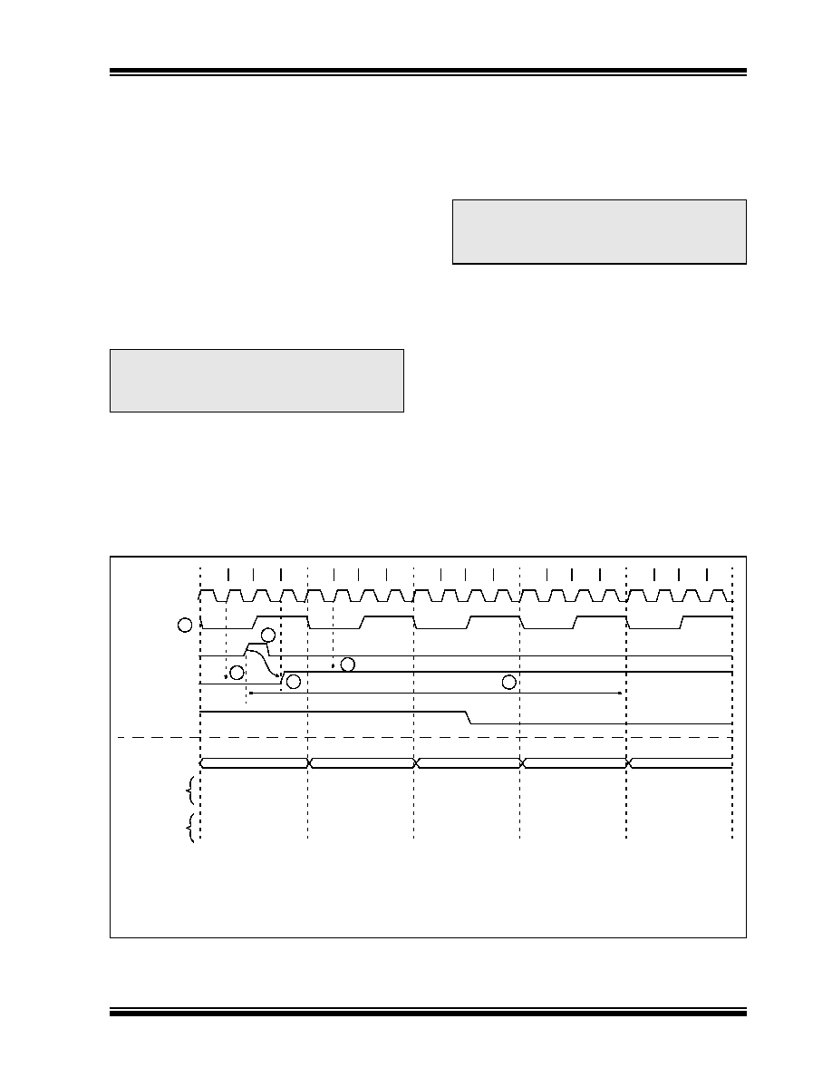
FIGURE 10-11:
INT PIN INTERRUPT TIMING
Note:
The ANSEL (9Fh) and CMCON (19h)
registers must be initialized to configure an
analog channel as a digital input. Pins
configured as analog inputs will read ‘0’.
Note:
If a change on the I/O pin should occur
when the read operation is being executed
(start of the Q2 cycle), then the GPIF inter-
rupt flag may not get set.
Q2
Q1
Q3
Q4
Q2
Q1
Q3
Q4
Q2
Q1
Q3
Q4
Q2
Q1
Q3
Q4
Q2
Q1
Q3
Q4
OSC1
CLKOUT
INT pin
INTF Flag
(INTCON<1>)
GIE bit
(INTCON<7>)
INSTRUCTION FLOW
PC
Instruction
Fetched
Instruction
Executed
Interrupt Latency
PC
PC+1
0004h
0005h
Inst (0004h)
Inst (0005h)
Dummy Cycle
Inst (PC)
Inst (PC+1)
Inst (PC-1)
Inst (0004h)
Dummy Cycle
Inst (PC)
—
1
4
5
1
2
3
Note
1: INTF flag is sampled here (every Q1).
2: Asynchronous interrupt latency = 3-4 T
CY. Synchronous latency = 3 TCY, where TCY = instruction cycle time. Latency
is the same whether Inst (PC) is a single cycle or a 2-cycle instruction.
3: CLKOUT is available only in RC Oscillator mode.
4: For minimum width of INT pulse, refer to AC specs.
5: INTF is enabled to be set any time during the Q4-Q1 cycles.
相关PDF资料 |
PDF描述 |
|---|---|
| RFPIC12F675H-E/SS | 8-BIT, FLASH, 20 MHz, RISC MICROCONTROLLER, PDSO20 |
| RH80530GZ001512 | 32-BIT, 1000 MHz, MICROPROCESSOR, CPGA478 |
| RH80530GZ009512 | 32-BIT, 1200 MHz, MICROPROCESSOR, CPGA478 |
| RJ80530GZ004512 | 32-BIT, 1066 MHz, MICROPROCESSOR, PBGA479 |
| RH80530GZ004512 | 32-BIT, 1066 MHz, MICROPROCESSOR, CPGA478 |
相关代理商/技术参数 |
参数描述 |
|---|---|
| RFPIC12F675K-I/SS | 功能描述:射频微控制器 - MCU 290-350MHz UHF ASK/FSK Transmitter RoHS:否 制造商:Silicon Labs 核心:8051 处理器系列:Si100x 数据总线宽度:8 bit 最大时钟频率:24 MHz 程序存储器大小:64 KB 数据 RAM 大小:4 KB 片上 ADC:Yes 工作电源电压:1.8 V to 3.6 V 工作温度范围:- 40 C to + 85 C 封装 / 箱体:LGA-42 安装风格:SMD/SMT 封装:Tube |
| RFPIC12F675KT-I/SS | 功能描述:射频微控制器 - MCU 1 KB Flash FSK ASK RoHS:否 制造商:Silicon Labs 核心:8051 处理器系列:Si100x 数据总线宽度:8 bit 最大时钟频率:24 MHz 程序存储器大小:64 KB 数据 RAM 大小:4 KB 片上 ADC:Yes 工作电源电压:1.8 V to 3.6 V 工作温度范围:- 40 C to + 85 C 封装 / 箱体:LGA-42 安装风格:SMD/SMT 封装:Tube |
| RFPMV00 | 制造商:Carlo Gavazzi 功能描述:RSBT ALARM RELAY OUTPUT MODULE |
| RF-PP12/23 | 制造商:Cembre 功能描述:F-CRIMP,BLADE,RED,PP12/23 |
| RFP-QD10 | 功能描述:烙铁 Cartridge Quad PLCC-52 Chip Pkg RoHS:否 制造商:Weller 产品:Soldering Stations 类型:Digital, Iron, Stand, Cleaner 瓦特:50 W 最大温度:+ 850 F 电缆类型:US Cord Included |
发布紧急采购,3分钟左右您将得到回复。