- 您现在的位置:买卖IC网 > PDF目录69321 > RFPIC12F675K-E/SS 8-BIT, FLASH, 20 MHz, RISC MICROCONTROLLER, PDSO20 PDF资料下载
参数资料
| 型号: | RFPIC12F675K-E/SS |
| 元件分类: | 微控制器/微处理器 |
| 英文描述: | 8-BIT, FLASH, 20 MHz, RISC MICROCONTROLLER, PDSO20 |
| 封装: | 0.209 INCH, PLASTIC, MO-150, SSOP-20 |
| 文件页数: | 78/123页 |
| 文件大小: | 5438K |
| 代理商: | RFPIC12F675K-E/SS |
第1页第2页第3页第4页第5页第6页第7页第8页第9页第10页第11页第12页第13页第14页第15页第16页第17页第18页第19页第20页第21页第22页第23页第24页第25页第26页第27页第28页第29页第30页第31页第32页第33页第34页第35页第36页第37页第38页第39页第40页第41页第42页第43页第44页第45页第46页第47页第48页第49页第50页第51页第52页第53页第54页第55页第56页第57页第58页第59页第60页第61页第62页第63页第64页第65页第66页第67页第68页第69页第70页第71页第72页第73页第74页第75页第76页第77页当前第78页第79页第80页第81页第82页第83页第84页第85页第86页第87页第88页第89页第90页第91页第92页第93页第94页第95页第96页第97页第98页第99页第100页第101页第102页第103页第104页第105页第106页第107页第108页第109页第110页第111页第112页第113页第114页第115页第116页第117页第118页第119页第120页第121页第122页第123页
rfPIC12F675
DS70091A-page 56
Preliminary
2003 Microchip Technology Inc.
10.1
Configuration Bits
The configuration bits can be programmed (read as '0'),
or left unprogrammed (read as '1') to select various
device configurations, as shown in Register 10-1.
These bits are mapped in program memory location
2007h.
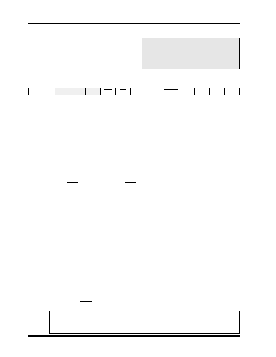
REGISTER 10-1:
CONFIG — CONFIGURATION WORD (ADDRESS: 2007h)
Note:
Address 2007h is beyond the user program
memory space. It belongs to the special
configuration
memory
space
(2000h -
3FFFh), which can be accessed only during
programming. See rfPIC12F675 Program-
ming Specification for more information.
R/P-1 R/P-1
U-0
R/P-1
BG1
BG0
—
CPD
CP
BODEN MCLRE PWRTE WDTE F0SC2 F0SC1 F0SC0
bit 13
bit 0
bit 13-12
BG1:BG0: Bandgap Calibration bits for BOD and POR voltage(1)
00 = Lowest bandgap voltage
11 = Highest bandgap voltage
bit 11-9
Unimplemented: Read as ‘0’
bit 8
CPD: Data Code Protection bit(2)
1 = Data memory code protection is disabled
0 = Data memory code protection is enabled
bit 7
CP: Code Protection bit(3)
1 = Program Memory code protection is disabled
0 = Program Memory code protection is enabled
bit 6
BODEN: Brown-out Detect Enable bit(4)
1 = BOD enabled
0 = BOD disabled
bit 5
MCLRE: GP3/MCLR pin function select(5)
1 = GP3/MCLR pin function is MCLR
0 = GP3/MCLR pin function is digital I/O, MCLR internally tied to VDD
bit 4
PWRTE: Power-up Timer Enable bit
1 = PWRT disabled
0 = PWRT enabled
bit 3
WDTE: Watchdog Timer Enable bit
1 = WDT enabled
0 = WDT disabled
bit 2-0
FOSC2:FOSC0: Oscillator Selection bits
111 = RC oscillator: CLKOUT function on GP4/OSC2/CLKOUT pin, RC on GP5/OSC1/CLKIN
110 = RC oscillator: I/O function on GP4/OSC2/CLKOUT pin, RC on GP5/OSC1/CLKIN
101 = INTOSC oscillator: CLKOUT function on GP4/OSC2/CLKOUT pin, I/O function on GP5/OSC1/CLKIN
100 = INTOSC oscillator: I/O function on GP4/OSC2/CLKOUT pin, I/O function on GP5/OSC1/CLKIN
011 = EC: I/O function on GP4/OSC2/CLKOUT pin, CLKIN on GP5/OSC1/CLKIN
010 = HS oscillator: High speed crystal/resonator on GP4/OSC2/CLKOUT and GP5/OSC1/CLKIN
001 = XT oscillator: Crystal/resonator on GP4/OSC2/CLKOUT and GP5/OSC1/CLKIN
000 = LP oscillator: Low power crystal on GP4/OSC2/CLKOUT and GP5/OSC1/CLKIN
Note 1: The Bandgap Calibration bits are factory programmed and must be read and saved prior to erasing
the device as specified in the rfPIC12F675 Programming Specification. These bits are reflected in
an export of the configuration word. Microchip Development Tools maintain all calibration bits to
factory settings.
2: The entire data EEPROM will be erased when the code protection is turned off.
3: The entire program memory will be erased, including OSCCAL value, when the code protection is
turned off.
4: Enabling Brown-out Detect does not automatically enable Power-up Timer.
5: When MCLR is asserted in INTOSC or RC mode, the internal clock oscillator is disabled.
Legend:
P = Programmed using ICSP
R = Readable bit
W = Writable bit
U = Unimplemented bit, read as ‘0’
-n = Value at POR
1 = bit is set
0 = bit is cleared
x = bit is unknown
相关PDF资料 |
PDF描述 |
|---|---|
| RFPIC12F675H-E/SS | 8-BIT, FLASH, 20 MHz, RISC MICROCONTROLLER, PDSO20 |
| RH80530GZ001512 | 32-BIT, 1000 MHz, MICROPROCESSOR, CPGA478 |
| RH80530GZ009512 | 32-BIT, 1200 MHz, MICROPROCESSOR, CPGA478 |
| RJ80530GZ004512 | 32-BIT, 1066 MHz, MICROPROCESSOR, PBGA479 |
| RH80530GZ004512 | 32-BIT, 1066 MHz, MICROPROCESSOR, CPGA478 |
相关代理商/技术参数 |
参数描述 |
|---|---|
| RFPIC12F675K-I/SS | 功能描述:射频微控制器 - MCU 290-350MHz UHF ASK/FSK Transmitter RoHS:否 制造商:Silicon Labs 核心:8051 处理器系列:Si100x 数据总线宽度:8 bit 最大时钟频率:24 MHz 程序存储器大小:64 KB 数据 RAM 大小:4 KB 片上 ADC:Yes 工作电源电压:1.8 V to 3.6 V 工作温度范围:- 40 C to + 85 C 封装 / 箱体:LGA-42 安装风格:SMD/SMT 封装:Tube |
| RFPIC12F675KT-I/SS | 功能描述:射频微控制器 - MCU 1 KB Flash FSK ASK RoHS:否 制造商:Silicon Labs 核心:8051 处理器系列:Si100x 数据总线宽度:8 bit 最大时钟频率:24 MHz 程序存储器大小:64 KB 数据 RAM 大小:4 KB 片上 ADC:Yes 工作电源电压:1.8 V to 3.6 V 工作温度范围:- 40 C to + 85 C 封装 / 箱体:LGA-42 安装风格:SMD/SMT 封装:Tube |
| RFPMV00 | 制造商:Carlo Gavazzi 功能描述:RSBT ALARM RELAY OUTPUT MODULE |
| RF-PP12/23 | 制造商:Cembre 功能描述:F-CRIMP,BLADE,RED,PP12/23 |
| RFP-QD10 | 功能描述:烙铁 Cartridge Quad PLCC-52 Chip Pkg RoHS:否 制造商:Weller 产品:Soldering Stations 类型:Digital, Iron, Stand, Cleaner 瓦特:50 W 最大温度:+ 850 F 电缆类型:US Cord Included |
发布紧急采购,3分钟左右您将得到回复。