- 您现在的位置:买卖IC网 > PDF目录69321 > RFPIC12F675K-E/SS 8-BIT, FLASH, 20 MHz, RISC MICROCONTROLLER, PDSO20 PDF资料下载
参数资料
| 型号: | RFPIC12F675K-E/SS |
| 元件分类: | 微控制器/微处理器 |
| 英文描述: | 8-BIT, FLASH, 20 MHz, RISC MICROCONTROLLER, PDSO20 |
| 封装: | 0.209 INCH, PLASTIC, MO-150, SSOP-20 |
| 文件页数: | 60/123页 |
| 文件大小: | 5438K |
| 代理商: | RFPIC12F675K-E/SS |
第1页第2页第3页第4页第5页第6页第7页第8页第9页第10页第11页第12页第13页第14页第15页第16页第17页第18页第19页第20页第21页第22页第23页第24页第25页第26页第27页第28页第29页第30页第31页第32页第33页第34页第35页第36页第37页第38页第39页第40页第41页第42页第43页第44页第45页第46页第47页第48页第49页第50页第51页第52页第53页第54页第55页第56页第57页第58页第59页当前第60页第61页第62页第63页第64页第65页第66页第67页第68页第69页第70页第71页第72页第73页第74页第75页第76页第77页第78页第79页第80页第81页第82页第83页第84页第85页第86页第87页第88页第89页第90页第91页第92页第93页第94页第95页第96页第97页第98页第99页第100页第101页第102页第103页第104页第105页第106页第107页第108页第109页第110页第111页第112页第113页第114页第115页第116页第117页第118页第119页第120页第121页第122页第123页
2003 Microchip Technology Inc.
Preliminary
DS70091A-page 39
rfPIC12F675
7.0
ANALOG-TO-DIGITAL
CONVERTER (A/D) MODULE
The analog-to-digital converter (A/D) allows conversion
of an analog input signal to a 10-bit binary representa-
tion of that signal. The rfPIC12F675 has four analog
inputs, multiplexed into one sample and hold circuit.
The output of the sample and hold is connected to the
input of the converter. The converter generates a
binary result via successive approximation and stores
the result in a 10-bit register. The voltage reference
used in the conversion is software selectable to either
V
shows the block diagram of the A/D.
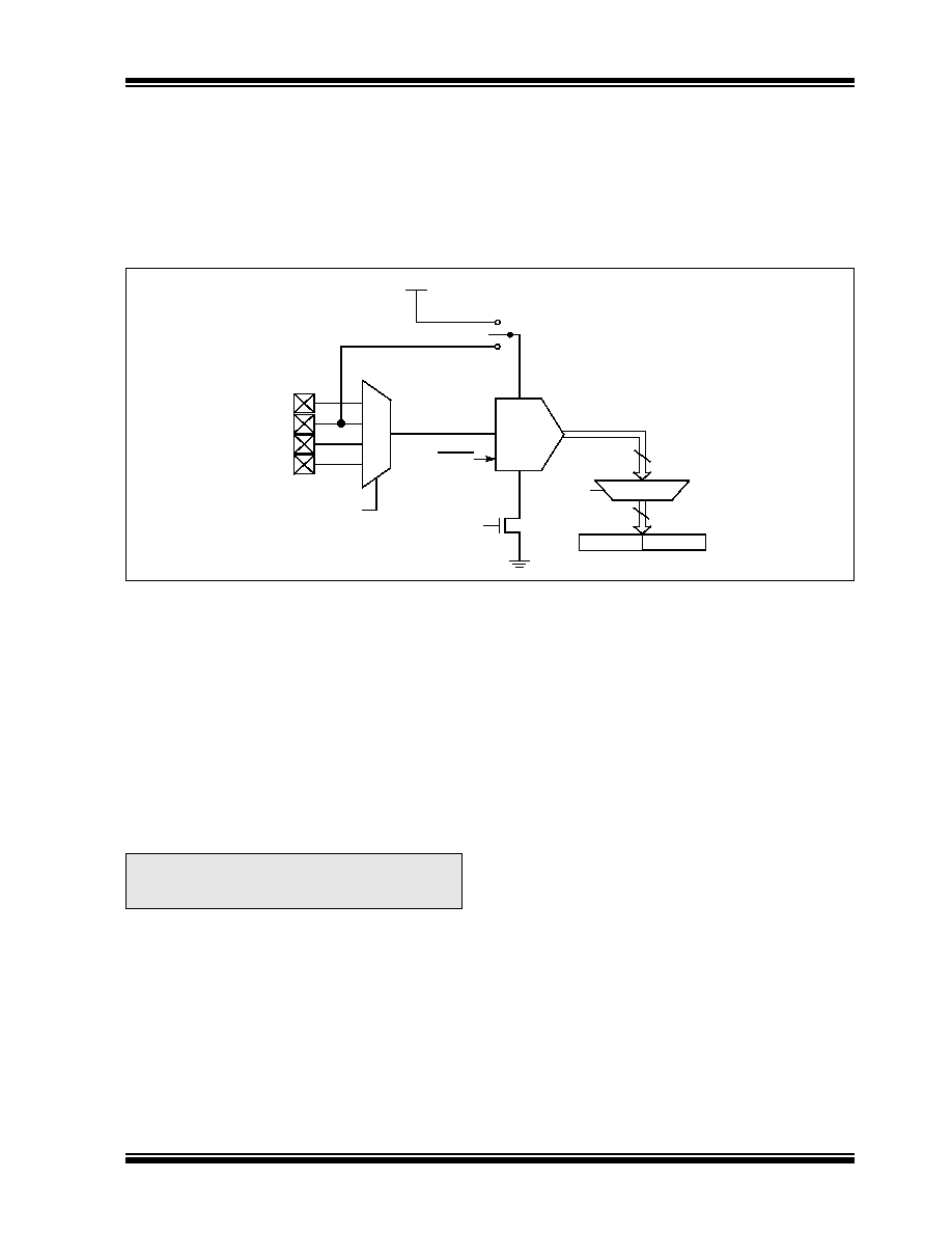
FIGURE 7-1:
A/D BLOCK DIAGRAM
7.1
A/D Configuration and Operation
There are two registers available to control the
functionality of the A/D module:
1.
ADCON0 (Register 7-1)
2.
ANSEL (Register 7-2)
7.1.1
ANALOG PORT PINS
The ANS3:ANS0 bits (ANSEL<3:0>) and the TRISIO
bits control the operation of the A/D port pins. Set the
corresponding TRISIO bits to set the pin output driver
to its high impedance state. Likewise, set the
corresponding ANS bit to disable the digital input
buffer.
7.1.2
CHANNEL SELECTION
There are four analog channels, AN0 through AN3. The
CHS1:CHS0
bits
(ADCON0<3:2>)
control
which
channel is connected to the sample and hold circuit.
7.1.3
VOLTAGE REFERENCE
There are two options for the voltage reference to the
A/D converter: either V
DD is used, or an analog voltage
applied to V
REF is used. The VCFG bit (ADCON0<6>)
controls the voltage reference selection. If VCFG is set,
then the voltage on the V
REF pin is the reference;
otherwise, V
DD is the reference.
7.1.4
CONVERSION CLOCK
The A/D conversion cycle requires 11 T
AD. The source
of the conversion clock is software selectable via the
ADCS bits (ANSEL<6:4>). There are seven possible
clock options:
F
OSC/2
F
OSC/4
F
OSC/8
F
OSC/16
F
OSC/32
F
OSC/64
F
RC (dedicated internal RC oscillator)
For correct conversion, the A/D conversion clock
(1/T
AD) must be selected to ensure a minimum TAD of
1.6
selected frequencies.
GP0/AN0
ADC
GP1/AN1/V
REF
GP2/AN2
GP4/AN3
V
DD
V
REF
ADON
GO/DONE
VCFG = 1
VCFG = 0
CHS1:CHS0
ADRESH
ADRESL
10
ADFM
V
SS
Note:
Analog voltages on any pin that is defined
as a digital input may cause the input
buffer to conduct excess current.
相关PDF资料 |
PDF描述 |
|---|---|
| RFPIC12F675H-E/SS | 8-BIT, FLASH, 20 MHz, RISC MICROCONTROLLER, PDSO20 |
| RH80530GZ001512 | 32-BIT, 1000 MHz, MICROPROCESSOR, CPGA478 |
| RH80530GZ009512 | 32-BIT, 1200 MHz, MICROPROCESSOR, CPGA478 |
| RJ80530GZ004512 | 32-BIT, 1066 MHz, MICROPROCESSOR, PBGA479 |
| RH80530GZ004512 | 32-BIT, 1066 MHz, MICROPROCESSOR, CPGA478 |
相关代理商/技术参数 |
参数描述 |
|---|---|
| RFPIC12F675K-I/SS | 功能描述:射频微控制器 - MCU 290-350MHz UHF ASK/FSK Transmitter RoHS:否 制造商:Silicon Labs 核心:8051 处理器系列:Si100x 数据总线宽度:8 bit 最大时钟频率:24 MHz 程序存储器大小:64 KB 数据 RAM 大小:4 KB 片上 ADC:Yes 工作电源电压:1.8 V to 3.6 V 工作温度范围:- 40 C to + 85 C 封装 / 箱体:LGA-42 安装风格:SMD/SMT 封装:Tube |
| RFPIC12F675KT-I/SS | 功能描述:射频微控制器 - MCU 1 KB Flash FSK ASK RoHS:否 制造商:Silicon Labs 核心:8051 处理器系列:Si100x 数据总线宽度:8 bit 最大时钟频率:24 MHz 程序存储器大小:64 KB 数据 RAM 大小:4 KB 片上 ADC:Yes 工作电源电压:1.8 V to 3.6 V 工作温度范围:- 40 C to + 85 C 封装 / 箱体:LGA-42 安装风格:SMD/SMT 封装:Tube |
| RFPMV00 | 制造商:Carlo Gavazzi 功能描述:RSBT ALARM RELAY OUTPUT MODULE |
| RF-PP12/23 | 制造商:Cembre 功能描述:F-CRIMP,BLADE,RED,PP12/23 |
| RFP-QD10 | 功能描述:烙铁 Cartridge Quad PLCC-52 Chip Pkg RoHS:否 制造商:Weller 产品:Soldering Stations 类型:Digital, Iron, Stand, Cleaner 瓦特:50 W 最大温度:+ 850 F 电缆类型:US Cord Included |
发布紧急采购,3分钟左右您将得到回复。