- 您现在的位置:买卖IC网 > PDF目录69321 > RFPIC12F675K-E/SS 8-BIT, FLASH, 20 MHz, RISC MICROCONTROLLER, PDSO20 PDF资料下载
参数资料
| 型号: | RFPIC12F675K-E/SS |
| 元件分类: | 微控制器/微处理器 |
| 英文描述: | 8-BIT, FLASH, 20 MHz, RISC MICROCONTROLLER, PDSO20 |
| 封装: | 0.209 INCH, PLASTIC, MO-150, SSOP-20 |
| 文件页数: | 67/123页 |
| 文件大小: | 5438K |
| 代理商: | RFPIC12F675K-E/SS |
第1页第2页第3页第4页第5页第6页第7页第8页第9页第10页第11页第12页第13页第14页第15页第16页第17页第18页第19页第20页第21页第22页第23页第24页第25页第26页第27页第28页第29页第30页第31页第32页第33页第34页第35页第36页第37页第38页第39页第40页第41页第42页第43页第44页第45页第46页第47页第48页第49页第50页第51页第52页第53页第54页第55页第56页第57页第58页第59页第60页第61页第62页第63页第64页第65页第66页当前第67页第68页第69页第70页第71页第72页第73页第74页第75页第76页第77页第78页第79页第80页第81页第82页第83页第84页第85页第86页第87页第88页第89页第90页第91页第92页第93页第94页第95页第96页第97页第98页第99页第100页第101页第102页第103页第104页第105页第106页第107页第108页第109页第110页第111页第112页第113页第114页第115页第116页第117页第118页第119页第120页第121页第122页第123页
rfPIC12F675
DS70091A-page 46
Preliminary
2003 Microchip Technology Inc.
8.1
EEADR
The EEADR register can address up to a maximum of
128 bytes of data EEPROM. Only seven of the eight
bits in the register (EEADR<6:0>) are required. The
MSb (bit 7) is ignored.
The upper bit should always be ‘0’ to remain upward
compatible with devices that have more data EEPROM
memory.
8.2
EECON1 AND EECON2
REGISTERS
EECON1 is the control register with four low order bits
physically implemented. The upper four bits are non-
implemented and read as '0's.
Control bits RD and WR initiate read and write,
respectively. These bits cannot be cleared, only set, in
software. They are cleared in hardware at completion
of the read or write operation. The inability to clear the
WR bit in software prevents the accidental, premature
termination of a write operation.
The WREN bit, when set, will allow a write operation.
On power-up, the WREN bit is clear. The WRERR bit is
set when a write operation is interrupted by a MCLR
Reset, or a WDT Time-out Reset during normal opera-
tion. In these situations, following RESET, the user can
check the WRERR bit, clear it, and rewrite the location.
The data and address will be cleared, therefore, the
EEDATA and EEADR registers will need to be re-
initialized.
Interrupt flag bit EEIF in the PIR1 register is set when
write is complete. This bit must be cleared in software.
EECON2 is not a physical register. Reading EECON2
will read all '0's. The EECON2 register is used
exclusively in the Data EEPROM write sequence.
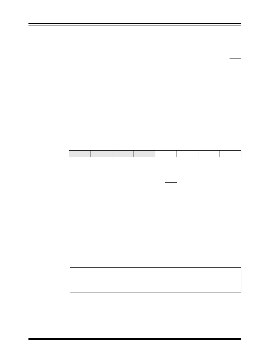
REGISTER 8-3:
EECON1 — EEPROM CONTROL REGISTER (ADDRESS: 9Ch)
U-0
R/W-x
R/W-0
R/S-0
—
WRERR
WREN
WR
RD
bit 7
bit 0
bit 7-4
Unimplemented: Read as ‘0’
bit 3
WRERR: EEPROM Error Flag bit
1 =A write operation is prematurely terminated (any MCLR Reset, any WDT Reset during
normal operation or BOD detect)
0 =The write operation completed
bit 2
WREN: EEPROM Write Enable bit
1 = Allows write cycles
0 = Inhibits write to the data EEPROM
bit 1
WR: Write Control bit
1 = Initiates a write cycle (The bit is cleared by hardware once write is complete. The WR bit
can only be set, not cleared, in software.)
0 = Write cycle to the data EEPROM is complete
bit 0
RD: Read Control bit
1 = Initiates an EEPROM read (Read takes one cycle. RD is cleared in hardware. The RD bit
can only be set, not cleared, in software.)
0 = Does not initiate an EEPROM read
Legend:
S = Bit can only be set
R = Readable bit
W = Writable bit
U = Unimplemented bit, read as ‘0’
- n = Value at POR
’1’ = Bit is set
’0’ = Bit is cleared
x = Bit is unknown
相关PDF资料 |
PDF描述 |
|---|---|
| RFPIC12F675H-E/SS | 8-BIT, FLASH, 20 MHz, RISC MICROCONTROLLER, PDSO20 |
| RH80530GZ001512 | 32-BIT, 1000 MHz, MICROPROCESSOR, CPGA478 |
| RH80530GZ009512 | 32-BIT, 1200 MHz, MICROPROCESSOR, CPGA478 |
| RJ80530GZ004512 | 32-BIT, 1066 MHz, MICROPROCESSOR, PBGA479 |
| RH80530GZ004512 | 32-BIT, 1066 MHz, MICROPROCESSOR, CPGA478 |
相关代理商/技术参数 |
参数描述 |
|---|---|
| RFPIC12F675K-I/SS | 功能描述:射频微控制器 - MCU 290-350MHz UHF ASK/FSK Transmitter RoHS:否 制造商:Silicon Labs 核心:8051 处理器系列:Si100x 数据总线宽度:8 bit 最大时钟频率:24 MHz 程序存储器大小:64 KB 数据 RAM 大小:4 KB 片上 ADC:Yes 工作电源电压:1.8 V to 3.6 V 工作温度范围:- 40 C to + 85 C 封装 / 箱体:LGA-42 安装风格:SMD/SMT 封装:Tube |
| RFPIC12F675KT-I/SS | 功能描述:射频微控制器 - MCU 1 KB Flash FSK ASK RoHS:否 制造商:Silicon Labs 核心:8051 处理器系列:Si100x 数据总线宽度:8 bit 最大时钟频率:24 MHz 程序存储器大小:64 KB 数据 RAM 大小:4 KB 片上 ADC:Yes 工作电源电压:1.8 V to 3.6 V 工作温度范围:- 40 C to + 85 C 封装 / 箱体:LGA-42 安装风格:SMD/SMT 封装:Tube |
| RFPMV00 | 制造商:Carlo Gavazzi 功能描述:RSBT ALARM RELAY OUTPUT MODULE |
| RF-PP12/23 | 制造商:Cembre 功能描述:F-CRIMP,BLADE,RED,PP12/23 |
| RFP-QD10 | 功能描述:烙铁 Cartridge Quad PLCC-52 Chip Pkg RoHS:否 制造商:Weller 产品:Soldering Stations 类型:Digital, Iron, Stand, Cleaner 瓦特:50 W 最大温度:+ 850 F 电缆类型:US Cord Included |
发布紧急采购,3分钟左右您将得到回复。