- 您现在的位置:买卖IC网 > PDF目录192300 > S29JL032J70TFI213 (SPANSION LLC) 2M X 16 FLASH 3V PROM, 70 ns, PDSO48 PDF资料下载
参数资料
| 型号: | S29JL032J70TFI213 |
| 厂商: | SPANSION LLC |
| 元件分类: | PROM |
| 英文描述: | 2M X 16 FLASH 3V PROM, 70 ns, PDSO48 |
| 封装: | LEAD FREE, MO-142(D)DD, TSOP-48 |
| 文件页数: | 28/63页 |
| 文件大小: | 1618K |
| 代理商: | S29JL032J70TFI213 |
第1页第2页第3页第4页第5页第6页第7页第8页第9页第10页第11页第12页第13页第14页第15页第16页第17页第18页第19页第20页第21页第22页第23页第24页第25页第26页第27页当前第28页第29页第30页第31页第32页第33页第34页第35页第36页第37页第38页第39页第40页第41页第42页第43页第44页第45页第46页第47页第48页第49页第50页第51页第52页第53页第54页第55页第56页第57页第58页第59页第60页第61页第62页第63页
34
S29JL032J
S29JL032J_00_05 August 24, 2011
Data
She e t
10.5.1
Unlock Bypass Command Sequence
The unlock bypass feature allows the system to program bytes or words to a bank faster than using the
standard program command sequence. The unlock bypass command sequence is initiated by first writing two
unlock cycles. This is followed by a third write cycle containing the unlock bypass command, 20h. That bank
then enters the unlock bypass mode. A two-cycle unlock bypass program command sequence is all that is
required to program in this mode. The first cycle in this sequence contains the unlock bypass program
command, A0h; the second cycle contains the program address and data. Additional data is programmed in
the same manner. This mode dispenses with the initial two unlock cycles required in the standard program
command sequence, resulting in faster total programming time. Table 10.1 on page 38 shows the
requirements for the command sequence.
During the unlock bypass mode, only the Unlock Bypass Program and Unlock Bypass Reset commands are
valid. To exit the unlock bypass mode, the system must issue the two-cycle unlock bypass reset command
sequence. (Table 10.1 on page 38).
The device offers accelerated program operations through the WP#/ACC pin. When the system asserts VHH
on the WP#/ACC pin, the device automatically enters the Unlock Bypass mode. The system may then write
the two-cycle Unlock Bypass program command sequence. The device uses the higher voltage on the WP#/
ACC pin to accelerate the operation. Note that the WP#/ACC pin must not be at VHH for any operation other
than accelerated programming, or device damage may result. In addition, the WP#/ACC pin must not be left
floating or unconnected; inconsistent behavior of the device may result.
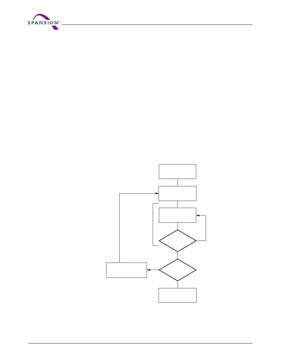
Figure 10.1 illustrates the algorithm for the program operation. Refer to Erase and Program Operations
on page 51 for parameters, and Figure 17.5 on page 52 for timing diagrams.
Figure 10.1 Program Operation
Note:
See Table 10.1 on page 38 for program command sequence.
START
Write Program
Command Sequence
Data Poll
from System
Verify Data?
No
Yes
Last Address?
No
Yes
Programming
Completed
Increment Address
Embedded
Program
algorithm
in progress
相关PDF资料 |
PDF描述 |
|---|---|
| S29PL032J65BFI150 | 2M X 16 FLASH 3V PROM, 65 ns, PBGA56 |
| S29PL127J70BFI000 | 8M X 16 FLASH 3V PROM, 70 ns, PBGA80 |
| S29XS064R0PBHW010 | 4M X 16 FLASH 1.8V PROM, 80 ns, PBGA44 |
| S2C3R-1-12-H | 4000 MHz - 12000 MHz RF/MICROWAVE SGL POLE DOUBLE THROW SWITCH, 2 dB INSERTION LOSS |
| S2C5R-1-12-RC | 4000 MHz - 18000 MHz RF/MICROWAVE SGL POLE DOUBLE THROW SWITCH, 2.8 dB INSERTION LOSS |
相关代理商/技术参数 |
参数描述 |
|---|---|
| S29JL032J70TFI220 | 功能描述:闪存 32MB 闪存 3.0V 70ns Parallel NOR 闪存 RoHS:否 制造商:ON Semiconductor 数据总线宽度:1 bit 存储类型:Flash 存储容量:2 MB 结构:256 K x 8 定时类型: 接口类型:SPI 访问时间: 电源电压-最大:3.6 V 电源电压-最小:2.3 V 最大工作电流:15 mA 工作温度:- 40 C to + 85 C 安装风格:SMD/SMT 封装 / 箱体: 封装:Reel |
| S29JL032J70TFI310 | 功能描述:闪存 32MB 闪存 3.0V 70ns Parallel NOR 闪存 RoHS:否 制造商:ON Semiconductor 数据总线宽度:1 bit 存储类型:Flash 存储容量:2 MB 结构:256 K x 8 定时类型: 接口类型:SPI 访问时间: 电源电压-最大:3.6 V 电源电压-最小:2.3 V 最大工作电流:15 mA 工作温度:- 40 C to + 85 C 安装风格:SMD/SMT 封装 / 箱体: 封装:Reel |
| S29JL032J70TFI313 | 制造商:Spansion 功能描述: |
| S29JL032J70TFI320 | 功能描述:闪存 32Mb 3V 70ns Parallel NOR 闪存 RoHS:否 制造商:ON Semiconductor 数据总线宽度:1 bit 存储类型:Flash 存储容量:2 MB 结构:256 K x 8 定时类型: 接口类型:SPI 访问时间: 电源电压-最大:3.6 V 电源电压-最小:2.3 V 最大工作电流:15 mA 工作温度:- 40 C to + 85 C 安装风格:SMD/SMT 封装 / 箱体: 封装:Reel |
| S29JL032J70TFI323 | 功能描述:闪存 32M, 3V, 70ns Parallel NOR 闪存 RoHS:否 制造商:ON Semiconductor 数据总线宽度:1 bit 存储类型:Flash 存储容量:2 MB 结构:256 K x 8 定时类型: 接口类型:SPI 访问时间: 电源电压-最大:3.6 V 电源电压-最小:2.3 V 最大工作电流:15 mA 工作温度:- 40 C to + 85 C 安装风格:SMD/SMT 封装 / 箱体: 封装:Reel |
发布紧急采购,3分钟左右您将得到回复。