- 您现在的位置:买卖IC网 > PDF目录192300 > S29JL032J70TFI213 (SPANSION LLC) 2M X 16 FLASH 3V PROM, 70 ns, PDSO48 PDF资料下载
参数资料
| 型号: | S29JL032J70TFI213 |
| 厂商: | SPANSION LLC |
| 元件分类: | PROM |
| 英文描述: | 2M X 16 FLASH 3V PROM, 70 ns, PDSO48 |
| 封装: | LEAD FREE, MO-142(D)DD, TSOP-48 |
| 文件页数: | 32/63页 |
| 文件大小: | 1618K |
| 代理商: | S29JL032J70TFI213 |
第1页第2页第3页第4页第5页第6页第7页第8页第9页第10页第11页第12页第13页第14页第15页第16页第17页第18页第19页第20页第21页第22页第23页第24页第25页第26页第27页第28页第29页第30页第31页当前第32页第33页第34页第35页第36页第37页第38页第39页第40页第41页第42页第43页第44页第45页第46页第47页第48页第49页第50页第51页第52页第53页第54页第55页第56页第57页第58页第59页第60页第61页第62页第63页
38
S29JL032J
S29JL032J_00_05 August 24, 2011
Data
She e t
Legend:
X = Don’t care
RA = Address of the memory location to be read.
RD = Data read from location RA during read operation.
PA = Address of the memory location to be programmed. Addresses latch on the falling edge of the WE# or CE# pulse, whichever happens later.
PD = Data to be programmed at location PA. Data latches on the rising edge of WE# or CE# pulse, whichever happens first.
SA = Address of the sector to be verified (in autoselect mode) or erased. Address bits A20–A12 uniquely select any sector.
Refer to Table 8.3 on page 18 and Table 8.4 on page 20 for information on sector addresses.
BA = Address of the bank that is being switched to autoselect mode, is in bypass mode, or is being erased. A20–A18 uniquely select a bank.
Notes:
1. See Table 8.1 on page 14 for description of bus operations.
2. All values are in hexadecimal.
3. Except for the read cycle and the fourth, fifth, and sixth cycle of the autoselect command sequence, all bus cycles are write cycles.
4. Data bits DQ15–DQ8 are don’t care in command sequences, except for RD and PD.
5. Unless otherwise noted, address bits A20–A11 are don’t cares for unlock and command cycles, unless SA or PA is required.
6. No unlock or command cycles required when bank is reading array data.
7. The Reset command is required to return to the read mode (or to the erase-suspend-read mode if previously in Erase Suspend) when a bank is in the autoselect
mode, or if DQ5 goes high (while the bank is providing status information).
8. The fourth cycle of the autoselect command sequence is a read cycle. The system must provide the bank address to obtain the manufacturer ID, device ID, or
Secured Silicon Region factory protect information. Data bits DQ15–DQ8 are don’t care. While reading the autoselect addresses, the bank address must be the
same until a reset command is given. See Autoselect Command Sequence on page 33 for more information.
9. For models 01, 02, the device ID must be read across the fourth, fifth, and sixth cycles.
10. The data is 82h for factory locked, 42h for customer locked, and 02h for not factory/customer locked.
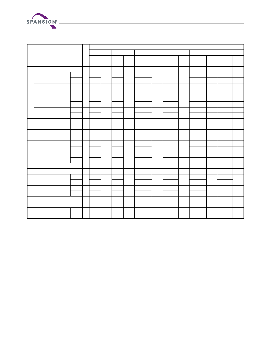
Table 10.1 S29JL032J Command Definitions
Command
Sequence
Cy
c
le
s
Bus Cycles (Notes 2–5)
First
Second
Third
Fourth
Fifth
Sixth
Addr
Data
Addr
Data
Addr
Data
Addr
Data
Addr
Data
Addr
Data
Read (Note 6)
1RA
RD
Reset (Note 7)
1XXX
F0
A
u
to
sel
e
ct
Manufacturer ID
Word
4
555
AA
2AA
55
(BA)555
90
(BA)X00
01
Byte
AAA
555
(BA)AAA
Device ID (Note 9)
Word
6
555
AA
2AA
55
(BA)555
90
(BA)X01
See
(BA)X0E
See
(BA)X0F
See
Byte
AAA
555
(BA)AAA
(BA)X02
(BA)X1C
(BA)X1E
Secured Silicon Region
Factory Protect (Note 10)
Word
4
555
AA
2AA
55
(BA)555
90
(BA)X03
82/02
Byte
AAA
555
(BA)AAA
(BA)X06
Boot Sector/Sector Block
Protect Verify (Note 11)
Word
4
555
AA
2AA
55
(BA)555
90
(SA)X02
00/01
Byte
AAA
555
(BA)AAA
(SA)X04
Enter Secured Silicon Region
Word
3
555
AA
2AA
55
555
88
Byte
AAA
555
AAA
Exit Secured Silicon Region
Word
4
555
AA
2AA
55
555
90
XXX
00
Byte
AAA
555
AAA
Program
Word
4
555
AA
2AA
55
555
A0
PA
PD
Byte
AAA
555
AAA
Unlock Bypass
Word
3
555
AA
2AA
55
555
20
Byte
AAA
555
AAA
Unlock Bypass Program (Note 12)
2
XXX
A0
PA
PD
Unlock Bypass Reset (Note 13)
2
XXX
90
XXX
00
Chip Erase
Word
6
555
AA
2AA
55
555
80
555
AA
2AA
55
555
10
Byte
AAA
555
AAA
555
AAA
Sector Erase (Note 17)
Word
6
555
AA
2AA
55
555
80
555
AA
2AA
55
SA
30
Byte
AAA
555
AAA
555
Erase Suspend (Note 14)
1BA
B0
Erase Resume (Note 15)
1BA
30
CFI Query (Note 16)
Word
1
55
98
Byte
AA
相关PDF资料 |
PDF描述 |
|---|---|
| S29PL032J65BFI150 | 2M X 16 FLASH 3V PROM, 65 ns, PBGA56 |
| S29PL127J70BFI000 | 8M X 16 FLASH 3V PROM, 70 ns, PBGA80 |
| S29XS064R0PBHW010 | 4M X 16 FLASH 1.8V PROM, 80 ns, PBGA44 |
| S2C3R-1-12-H | 4000 MHz - 12000 MHz RF/MICROWAVE SGL POLE DOUBLE THROW SWITCH, 2 dB INSERTION LOSS |
| S2C5R-1-12-RC | 4000 MHz - 18000 MHz RF/MICROWAVE SGL POLE DOUBLE THROW SWITCH, 2.8 dB INSERTION LOSS |
相关代理商/技术参数 |
参数描述 |
|---|---|
| S29JL032J70TFI220 | 功能描述:闪存 32MB 闪存 3.0V 70ns Parallel NOR 闪存 RoHS:否 制造商:ON Semiconductor 数据总线宽度:1 bit 存储类型:Flash 存储容量:2 MB 结构:256 K x 8 定时类型: 接口类型:SPI 访问时间: 电源电压-最大:3.6 V 电源电压-最小:2.3 V 最大工作电流:15 mA 工作温度:- 40 C to + 85 C 安装风格:SMD/SMT 封装 / 箱体: 封装:Reel |
| S29JL032J70TFI310 | 功能描述:闪存 32MB 闪存 3.0V 70ns Parallel NOR 闪存 RoHS:否 制造商:ON Semiconductor 数据总线宽度:1 bit 存储类型:Flash 存储容量:2 MB 结构:256 K x 8 定时类型: 接口类型:SPI 访问时间: 电源电压-最大:3.6 V 电源电压-最小:2.3 V 最大工作电流:15 mA 工作温度:- 40 C to + 85 C 安装风格:SMD/SMT 封装 / 箱体: 封装:Reel |
| S29JL032J70TFI313 | 制造商:Spansion 功能描述: |
| S29JL032J70TFI320 | 功能描述:闪存 32Mb 3V 70ns Parallel NOR 闪存 RoHS:否 制造商:ON Semiconductor 数据总线宽度:1 bit 存储类型:Flash 存储容量:2 MB 结构:256 K x 8 定时类型: 接口类型:SPI 访问时间: 电源电压-最大:3.6 V 电源电压-最小:2.3 V 最大工作电流:15 mA 工作温度:- 40 C to + 85 C 安装风格:SMD/SMT 封装 / 箱体: 封装:Reel |
| S29JL032J70TFI323 | 功能描述:闪存 32M, 3V, 70ns Parallel NOR 闪存 RoHS:否 制造商:ON Semiconductor 数据总线宽度:1 bit 存储类型:Flash 存储容量:2 MB 结构:256 K x 8 定时类型: 接口类型:SPI 访问时间: 电源电压-最大:3.6 V 电源电压-最小:2.3 V 最大工作电流:15 mA 工作温度:- 40 C to + 85 C 安装风格:SMD/SMT 封装 / 箱体: 封装:Reel |
发布紧急采购,3分钟左右您将得到回复。