- 您现在的位置:买卖IC网 > PDF目录192300 > S29JL032J70TFI213 (SPANSION LLC) 2M X 16 FLASH 3V PROM, 70 ns, PDSO48 PDF资料下载
参数资料
| 型号: | S29JL032J70TFI213 |
| 厂商: | SPANSION LLC |
| 元件分类: | PROM |
| 英文描述: | 2M X 16 FLASH 3V PROM, 70 ns, PDSO48 |
| 封装: | LEAD FREE, MO-142(D)DD, TSOP-48 |
| 文件页数: | 39/63页 |
| 文件大小: | 1618K |
| 代理商: | S29JL032J70TFI213 |
第1页第2页第3页第4页第5页第6页第7页第8页第9页第10页第11页第12页第13页第14页第15页第16页第17页第18页第19页第20页第21页第22页第23页第24页第25页第26页第27页第28页第29页第30页第31页第32页第33页第34页第35页第36页第37页第38页当前第39页第40页第41页第42页第43页第44页第45页第46页第47页第48页第49页第50页第51页第52页第53页第54页第55页第56页第57页第58页第59页第60页第61页第62页第63页
44
S29JL032J
S29JL032J_00_05 August 24, 2011
Data
She e t
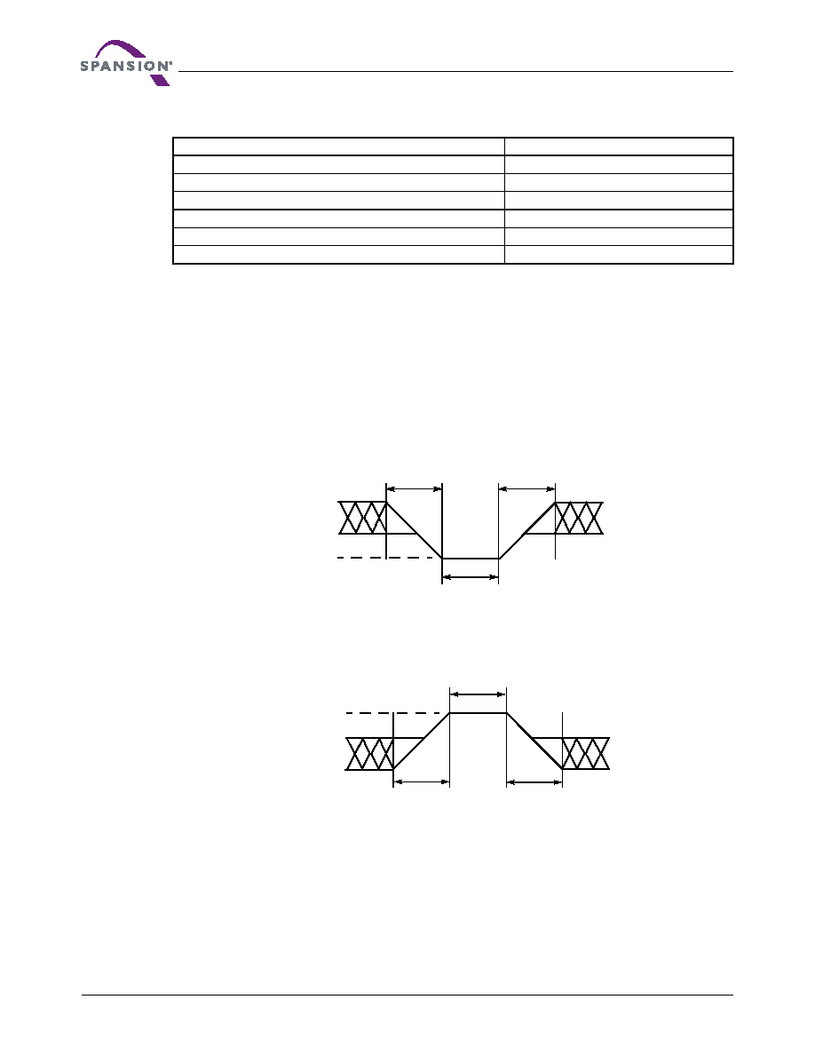
12. Absolute Maximum Ratings
Notes:
1. Minimum DC voltage on input or I/O pins is –0.5V. During voltage transitions, input or I/O pins may overshoot VSS to –2.0V for periods of
up to 20 ns. Maximum DC voltage on input or I/O pins is VCC +0.5V. See Figure 12.1 on page 44. During voltage transitions, input or I/O
2. Minimum DC input voltage on pins A9, OE#, RESET#, and WP#/ACC is –0.5V. During voltage transitions, A9, OE#, WP#/ACC, and
RESET# may overshoot VSS to –2.0V for periods of up to 20 ns. See Figure 12.1 on page 44. Maximum DC input voltage on pin A9 is
+12.5V which may overshoot to +14.0V for periods up to 20 ns. Maximum DC input voltage on WP#/ACC is +9.5V which may overshoot
to +12.0V for periods up to 20 ns.
3. No more than one output may be shorted to ground at a time. Duration of the short circuit should not be greater than one second.
4. Stresses above those listed under “Absolute Maximum Ratings” may cause permanent damage to the device. This is a stress rating only;
functional operation of the device at these or any other conditions above those indicated in the operational sections of this data sheet is
not implied. Exposure of the device to absolute maximum rating conditions for extended periods may affect device reliability.
Figure 12.1 Maximum Negative Overshoot Waveform
Figure 12.2 Maximum Positive Overshoot Waveform
Storage Temperature, Plastic Packages
–65°C to +150°C
Ambient Temperature with Power Applied
–65°C to +125°C
Voltage with Respect to Ground, VCC (Note 1)
–0.5V to +4.0V
A9 and RESET# (Note 2)
–0.5V to +12.5V
WP#/ACC
–0.5V to +9.5V
All other pins (Note 1)
–0.5V to VCC +0.5V
Output Short Circuit Current (Note 3)
200 mA
20 ns
+0.8V
–0.5V
20 ns
–2.0V
20 ns
VCC
+2.0V
VCC
+0.5V
20 ns
2.0V
相关PDF资料 |
PDF描述 |
|---|---|
| S29PL032J65BFI150 | 2M X 16 FLASH 3V PROM, 65 ns, PBGA56 |
| S29PL127J70BFI000 | 8M X 16 FLASH 3V PROM, 70 ns, PBGA80 |
| S29XS064R0PBHW010 | 4M X 16 FLASH 1.8V PROM, 80 ns, PBGA44 |
| S2C3R-1-12-H | 4000 MHz - 12000 MHz RF/MICROWAVE SGL POLE DOUBLE THROW SWITCH, 2 dB INSERTION LOSS |
| S2C5R-1-12-RC | 4000 MHz - 18000 MHz RF/MICROWAVE SGL POLE DOUBLE THROW SWITCH, 2.8 dB INSERTION LOSS |
相关代理商/技术参数 |
参数描述 |
|---|---|
| S29JL032J70TFI220 | 功能描述:闪存 32MB 闪存 3.0V 70ns Parallel NOR 闪存 RoHS:否 制造商:ON Semiconductor 数据总线宽度:1 bit 存储类型:Flash 存储容量:2 MB 结构:256 K x 8 定时类型: 接口类型:SPI 访问时间: 电源电压-最大:3.6 V 电源电压-最小:2.3 V 最大工作电流:15 mA 工作温度:- 40 C to + 85 C 安装风格:SMD/SMT 封装 / 箱体: 封装:Reel |
| S29JL032J70TFI310 | 功能描述:闪存 32MB 闪存 3.0V 70ns Parallel NOR 闪存 RoHS:否 制造商:ON Semiconductor 数据总线宽度:1 bit 存储类型:Flash 存储容量:2 MB 结构:256 K x 8 定时类型: 接口类型:SPI 访问时间: 电源电压-最大:3.6 V 电源电压-最小:2.3 V 最大工作电流:15 mA 工作温度:- 40 C to + 85 C 安装风格:SMD/SMT 封装 / 箱体: 封装:Reel |
| S29JL032J70TFI313 | 制造商:Spansion 功能描述: |
| S29JL032J70TFI320 | 功能描述:闪存 32Mb 3V 70ns Parallel NOR 闪存 RoHS:否 制造商:ON Semiconductor 数据总线宽度:1 bit 存储类型:Flash 存储容量:2 MB 结构:256 K x 8 定时类型: 接口类型:SPI 访问时间: 电源电压-最大:3.6 V 电源电压-最小:2.3 V 最大工作电流:15 mA 工作温度:- 40 C to + 85 C 安装风格:SMD/SMT 封装 / 箱体: 封装:Reel |
| S29JL032J70TFI323 | 功能描述:闪存 32M, 3V, 70ns Parallel NOR 闪存 RoHS:否 制造商:ON Semiconductor 数据总线宽度:1 bit 存储类型:Flash 存储容量:2 MB 结构:256 K x 8 定时类型: 接口类型:SPI 访问时间: 电源电压-最大:3.6 V 电源电压-最小:2.3 V 最大工作电流:15 mA 工作温度:- 40 C to + 85 C 安装风格:SMD/SMT 封装 / 箱体: 封装:Reel |
发布紧急采购,3分钟左右您将得到回复。