- 您现在的位置:买卖IC网 > PDF目录192300 > S29JL032J70TFI213 (SPANSION LLC) 2M X 16 FLASH 3V PROM, 70 ns, PDSO48 PDF资料下载
参数资料
| 型号: | S29JL032J70TFI213 |
| 厂商: | SPANSION LLC |
| 元件分类: | PROM |
| 英文描述: | 2M X 16 FLASH 3V PROM, 70 ns, PDSO48 |
| 封装: | LEAD FREE, MO-142(D)DD, TSOP-48 |
| 文件页数: | 35/63页 |
| 文件大小: | 1618K |
| 代理商: | S29JL032J70TFI213 |
第1页第2页第3页第4页第5页第6页第7页第8页第9页第10页第11页第12页第13页第14页第15页第16页第17页第18页第19页第20页第21页第22页第23页第24页第25页第26页第27页第28页第29页第30页第31页第32页第33页第34页当前第35页第36页第37页第38页第39页第40页第41页第42页第43页第44页第45页第46页第47页第48页第49页第50页第51页第52页第53页第54页第55页第56页第57页第58页第59页第60页第61页第62页第63页
40
S29JL032J
S29JL032J_00_05 August 24, 2011
Data
She e t
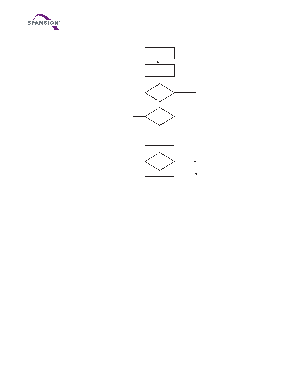
Figure 11.1 Data# Polling Algorithm
Notes:
1. VA = Valid address for programming. During a sector erase operation, a valid address is any sector address within the sector being
erased. During chip erase, a valid address is any non-protected sector address.
2. DQ7 should be rechecked even if DQ5 = “1” because DQ7 may change simultaneously with DQ5.
11.2
RY/BY#: Ready/Busy#
The RY/BY# is a dedicated, open-drain output pin which indicates whether an Embedded Algorithm is in
progress or complete. The RY/BY# status is valid after the rising edge of the final WE# pulse in the command
sequence. Since RY/BY# is an open-drain output, several RY/BY# pins can be tied together in parallel with a
pull-up resistor to VCC.
If the output is low (Busy), the device is actively erasing or programming. (This includes programming in the
Erase Suspend mode.) If the output is high (Ready), the device is in the read mode, the standby mode, or one
of the banks is in the erase-suspend-read mode.
Table 11.1 on page 43 shows the outputs for RY/BY#.
When DQ5 is set to “1”, RY/BY# will be in the BUSY state, or “0”.
11.3
DQ6: Toggle Bit I
Toggle Bit I on DQ6 indicates whether an Embedded Program or Erase algorithm is in progress or complete,
or whether the device has entered the Erase Suspend mode. Toggle Bit I may be read at any address, and is
valid after the rising edge of the final WE# pulse in the command sequence (prior to the program or erase
operation), and during the sector erase time-out.
相关PDF资料 |
PDF描述 |
|---|---|
| S29PL032J65BFI150 | 2M X 16 FLASH 3V PROM, 65 ns, PBGA56 |
| S29PL127J70BFI000 | 8M X 16 FLASH 3V PROM, 70 ns, PBGA80 |
| S29XS064R0PBHW010 | 4M X 16 FLASH 1.8V PROM, 80 ns, PBGA44 |
| S2C3R-1-12-H | 4000 MHz - 12000 MHz RF/MICROWAVE SGL POLE DOUBLE THROW SWITCH, 2 dB INSERTION LOSS |
| S2C5R-1-12-RC | 4000 MHz - 18000 MHz RF/MICROWAVE SGL POLE DOUBLE THROW SWITCH, 2.8 dB INSERTION LOSS |
相关代理商/技术参数 |
参数描述 |
|---|---|
| S29JL032J70TFI220 | 功能描述:闪存 32MB 闪存 3.0V 70ns Parallel NOR 闪存 RoHS:否 制造商:ON Semiconductor 数据总线宽度:1 bit 存储类型:Flash 存储容量:2 MB 结构:256 K x 8 定时类型: 接口类型:SPI 访问时间: 电源电压-最大:3.6 V 电源电压-最小:2.3 V 最大工作电流:15 mA 工作温度:- 40 C to + 85 C 安装风格:SMD/SMT 封装 / 箱体: 封装:Reel |
| S29JL032J70TFI310 | 功能描述:闪存 32MB 闪存 3.0V 70ns Parallel NOR 闪存 RoHS:否 制造商:ON Semiconductor 数据总线宽度:1 bit 存储类型:Flash 存储容量:2 MB 结构:256 K x 8 定时类型: 接口类型:SPI 访问时间: 电源电压-最大:3.6 V 电源电压-最小:2.3 V 最大工作电流:15 mA 工作温度:- 40 C to + 85 C 安装风格:SMD/SMT 封装 / 箱体: 封装:Reel |
| S29JL032J70TFI313 | 制造商:Spansion 功能描述: |
| S29JL032J70TFI320 | 功能描述:闪存 32Mb 3V 70ns Parallel NOR 闪存 RoHS:否 制造商:ON Semiconductor 数据总线宽度:1 bit 存储类型:Flash 存储容量:2 MB 结构:256 K x 8 定时类型: 接口类型:SPI 访问时间: 电源电压-最大:3.6 V 电源电压-最小:2.3 V 最大工作电流:15 mA 工作温度:- 40 C to + 85 C 安装风格:SMD/SMT 封装 / 箱体: 封装:Reel |
| S29JL032J70TFI323 | 功能描述:闪存 32M, 3V, 70ns Parallel NOR 闪存 RoHS:否 制造商:ON Semiconductor 数据总线宽度:1 bit 存储类型:Flash 存储容量:2 MB 结构:256 K x 8 定时类型: 接口类型:SPI 访问时间: 电源电压-最大:3.6 V 电源电压-最小:2.3 V 最大工作电流:15 mA 工作温度:- 40 C to + 85 C 安装风格:SMD/SMT 封装 / 箱体: 封装:Reel |
发布紧急采购,3分钟左右您将得到回复。