- 您现在的位置:买卖IC网 > PDF目录98143 > ST52510F3M6 (STMICROELECTRONICS) MICROCONTROLLER, PDSO20 PDF资料下载
参数资料
| 型号: | ST52510F3M6 |
| 厂商: | STMICROELECTRONICS |
| 元件分类: | 微控制器/微处理器 |
| 英文描述: | MICROCONTROLLER, PDSO20 |
| 封装: | SOP-20 |
| 文件页数: | 12/136页 |
| 文件大小: | 3335K |
| 代理商: | ST52510F3M6 |
第1页第2页第3页第4页第5页第6页第7页第8页第9页第10页第11页当前第12页第13页第14页第15页第16页第17页第18页第19页第20页第21页第22页第23页第24页第25页第26页第27页第28页第29页第30页第31页第32页第33页第34页第35页第36页第37页第38页第39页第40页第41页第42页第43页第44页第45页第46页第47页第48页第49页第50页第51页第52页第53页第54页第55页第56页第57页第58页第59页第60页第61页第62页第63页第64页第65页第66页第67页第68页第69页第70页第71页第72页第73页第74页第75页第76页第77页第78页第79页第80页第81页第82页第83页第84页第85页第86页第87页第88页第89页第90页第91页第92页第93页第94页第95页第96页第97页第98页第99页第100页第101页第102页第103页第104页第105页第106页第107页第108页第109页第110页第111页第112页第113页第114页第115页第116页第117页第118页第119页第120页第121页第122页第123页第124页第125页第126页第127页第128页第129页第130页第131页第132页第133页第134页第135页第136页
Obsolete
Product(s)
- Obsolete
Product(s)
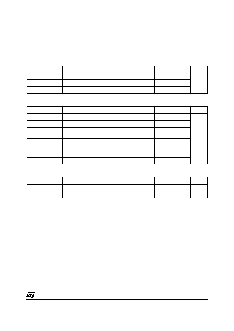
16.2 Absolute Maximum Ratings
Stresses above those listed as “absolute maximum ratings” may cause permanent damage to the device.
This is a stress rating only. Functional operation of the device under these conditions is not implied.
Exposure to maximum rating conditions for extended periods may affect device reliability.
Table 16.1 Voltage Characteristics
Symbol
Ratings
Max Values
Unit
VDD-VSS
Supply voltage
6.5
V
VIN
Input voltage on any pin 1) 2)
VSS-0.3 to VDD+0.3
VDESD
Electrostatic discharge voltage
2000
Table 16.2 Current Characteristics
Symbol
Ratings
Max Values
Unit
IVDD
Total current in VDD power lines (source)3)
100
mA
IVSS
Total current in VSS ground lines (sink)3)
100
IIO
Output current sunk by any standard I/O and control pin
20
Output current source by any I/Os and control pin
-20
Injected current on RESET pin
± 5
IINJ(PIN)2)
Injected current on OSCin and OSCout pins
± 5
Injected current on any other pin 4)
± 5
ΣIINJ(PIN)
Total Injected current (sum of all I/O and control pins) 4)
± 20
Table 16.3 Thermal Characteristics
Symbol
Ratings
Max Values
Unit
TSTG
Storage temperature range
-65 to +150
° C
TJ
Maximum junction temperature
150
Notes:
1. Connecting I/O Pins directly to VDD or VSS could damage the device if the unintentional internal reset
is generated or an unexpected change of I/O configuration occurs (for example, due to the corrupted
program counter). In order to guarantee safe operation, this connection has to be performed via a pull-
up or pull-down resistor (typical: 10K Ω for I/Os). Unused I/O pins must be tied in the same manner to
VDD or VSS according to their reset configuration.
2. When the current limitation is not possible, the VIN absolute maximum rating must be respected, other-
wise refer to IINJ(PIN) specification. A positive injection is induced by VIN>VDD while a negative injec-
tion is induced by VIN<VSS to IINJ(PIN) specification. A positive injection is VIN>VDD while a negative
injection is induced by VIN<VSS. Data by design.
3. All power (VDD) and ground (VSS) lines must always be connected to the external supply.
4. When several inputs are submitted to a current injection, the maximum
ΣIINJ(PIN) is the absolute sum of
the positive and negative injected currents (instantaneous values). Data by design.
相关PDF资料 |
PDF描述 |
|---|---|
| ST52E430B/D | 8-BIT, UVPROM, 20 MHz, MICROCONTROLLER, CDIP32 |
| ST52F510F1M6 | 8-BIT, FLASH, 24 MHz, MICROCONTROLLER, PDSO20 |
| ST52F510G0B6 | 8-BIT, FLASH, 24 MHz, MICROCONTROLLER, PDIP28 |
| ST52F513F0M6 | 8-BIT, FLASH, 24 MHz, MICROCONTROLLER, PDSO20 |
| ST52F513F1B6 | 8-BIT, FLASH, 24 MHz, MICROCONTROLLER, PDIP20 |
相关代理商/技术参数 |
参数描述 |
|---|---|
| ST52510G2 | 制造商:未知厂家 制造商全称:未知厂家 功能描述:8-BIT ICU WITH 10-BIT ADC. TWO TIMERS/PWM. I2C. SPI. SCI. UP TO 8K FLASH |
| ST52510G3 | 制造商:未知厂家 制造商全称:未知厂家 功能描述:8-BIT ICU WITH 10-BIT ADC. TWO TIMERS/PWM. I2C. SPI. SCI. UP TO 8K FLASH |
| ST52510K2 | 制造商:未知厂家 制造商全称:未知厂家 功能描述:8-BIT ICU WITH 10-BIT ADC. TWO TIMERS/PWM. I2C. SPI. SCI. UP TO 8K FLASH |
| ST52510K3 | 制造商:未知厂家 制造商全称:未知厂家 功能描述:8-BIT ICU WITH 10-BIT ADC. TWO TIMERS/PWM. I2C. SPI. SCI. UP TO 8K FLASH |
| ST52510Y2 | 制造商:未知厂家 制造商全称:未知厂家 功能描述:8-BIT ICU WITH 10-BIT ADC. TWO TIMERS/PWM. I2C. SPI. SCI. UP TO 8K FLASH |
发布紧急采购,3分钟左右您将得到回复。