- 您现在的位置:买卖IC网 > PDF目录98143 > ST52510F3M6 (STMICROELECTRONICS) MICROCONTROLLER, PDSO20 PDF资料下载
参数资料
| 型号: | ST52510F3M6 |
| 厂商: | STMICROELECTRONICS |
| 元件分类: | 微控制器/微处理器 |
| 英文描述: | MICROCONTROLLER, PDSO20 |
| 封装: | SOP-20 |
| 文件页数: | 8/136页 |
| 文件大小: | 3335K |
| 代理商: | ST52510F3M6 |
第1页第2页第3页第4页第5页第6页第7页当前第8页第9页第10页第11页第12页第13页第14页第15页第16页第17页第18页第19页第20页第21页第22页第23页第24页第25页第26页第27页第28页第29页第30页第31页第32页第33页第34页第35页第36页第37页第38页第39页第40页第41页第42页第43页第44页第45页第46页第47页第48页第49页第50页第51页第52页第53页第54页第55页第56页第57页第58页第59页第60页第61页第62页第63页第64页第65页第66页第67页第68页第69页第70页第71页第72页第73页第74页第75页第76页第77页第78页第79页第80页第81页第82页第83页第84页第85页第86页第87页第88页第89页第90页第91页第92页第93页第94页第95页第96页第97页第98页第99页第100页第101页第102页第103页第104页第105页第106页第107页第108页第109页第110页第111页第112页第113页第114页第115页第116页第117页第118页第119页第120页第121页第122页第123页第124页第125页第126页第127页第128页第129页第130页第131页第132页第133页第134页第135页第136页
Obsolete
Product(s)
- Obsolete
Product(s)
15.5 SPI Register Description
In the following sections describe the registers
used by the SPI.
15.5.1 SPI Configuration Registers.
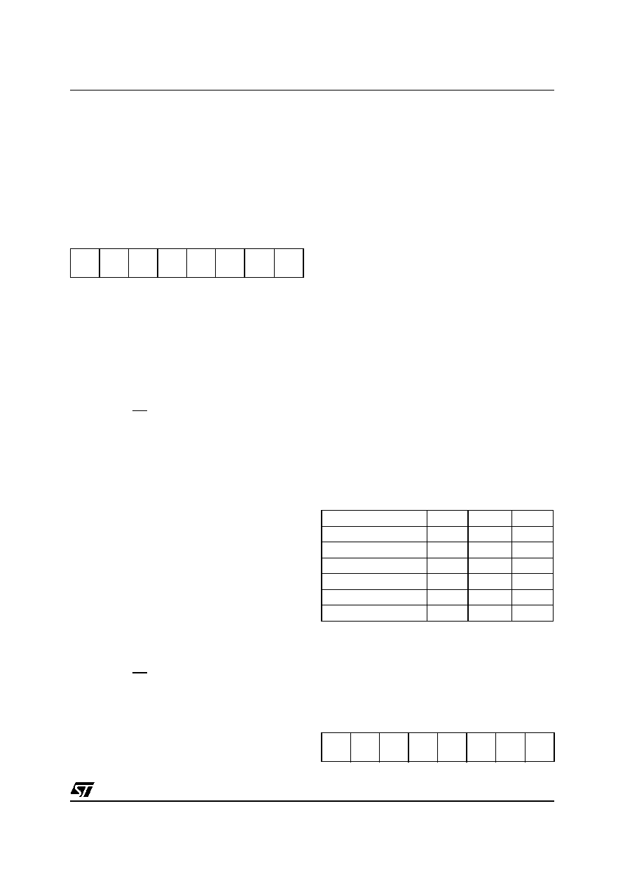
SPI Control Register (SPI_CR)
Configuration Register 20 (014h) Read/Write
Reset Value: 0000 0000 (00h)
Bit 7: SPIE Serial peripheral interrupt enable.
This bit is set and cleared by software.
0: Interrupt is inhibited
1: An SPI interrupt is generated whenever
SPIF=1 or MODF=1 in SPI_STATUS_CR
Bit 6: SPE Serial peripheral output enable.
This bit is set and cleared by software. It is
also cleared by hardware when, in master
mode, SS=0 (see Section 15.4.5 Master
0: I/O port connected to pins
1: SPI alternate functions connected to pins
Note: The SPE bit is cleared by reset, so the SPI
peripheral is not initially connected to the pins.
Bit 5: SPR2 Divider Enable.
This bit is set and cleared by software and it
is cleared by reset. It is used with the
SPR[1:0] bits to set the baud rate. Refer to
0: Divider by 2 enabled
1: Divider by 2 disabled
Note: This bit has no effect in slave mode.
Bit 4: MSTR Master/Slave mode select.
This bit is set and cleared by software. It is
also cleared by hardware when, in master
mode, SS=0 (see Section 15.4.5 Master
0: Slave mode is selected
1: Master mode is selected, the function of
the SCK pin changes from an input to an
output and the functions of the MISO and
MOSI pins are reversed.
Bit 3: CPOL Clock polarity.
This bit is set and cleared by software. This
bit determines the steady state of the serial
Clock. The CPOL bit affects both the master
and slave modes.
0: The steady state is a low value at the SCK
pin.
1: The steady state is a high value at the SCK
pin.
Note: SPI must be disabled by resetting the SPE
bit if CPOL is changed at the communication byte
boundaries.
Bit 2: CPHA Clock phase.
This bit is set and cleared by software.
0: The first clock transition is the first data
capture edge.
1: The second clock transition is the first
capture edge.
Bit 1-0: SPR1-SPR0 Serial peripheral rate.
These bits are set and cleared by software.
Used with the SPR2 bit, they select one of six
baud rates to be used as the serial clock
when the device is a master (see Table 15.1).
These 2 bits have no effect in slave mode.
Remark: It is recommended to write the SPI_CR
register after the SPI_STATUS_CR register when
working in master mode, vice versa when working
in slave mode.
1) This configuration is allowed only for master transmit, not for
master or slave receive.
SPI Control-Status Register (SPI_STATUS_CR)
Configuration Register 21 (015h) Read/Write
Reset Value: 0000 0000 (00h)
70
SPIE
SPE
SPR2
MSTR
CPOL
CPHA
SPR1
SPR0
Table 15.1 Serial Peripheral Baud Rate
Serial Clock
SPR2
SPR1
SPR0
fCKM/2
1)
10
0
fCKM/4
0
fCKM/8
0
1
fCKM/16
1
0
fCKM/32
0
1
0
fCKM/64
0
1
70
SPIF
WCOL
OR
MODF
-
SOD
SSM
SSI
相关PDF资料 |
PDF描述 |
|---|---|
| ST52E430B/D | 8-BIT, UVPROM, 20 MHz, MICROCONTROLLER, CDIP32 |
| ST52F510F1M6 | 8-BIT, FLASH, 24 MHz, MICROCONTROLLER, PDSO20 |
| ST52F510G0B6 | 8-BIT, FLASH, 24 MHz, MICROCONTROLLER, PDIP28 |
| ST52F513F0M6 | 8-BIT, FLASH, 24 MHz, MICROCONTROLLER, PDSO20 |
| ST52F513F1B6 | 8-BIT, FLASH, 24 MHz, MICROCONTROLLER, PDIP20 |
相关代理商/技术参数 |
参数描述 |
|---|---|
| ST52510G2 | 制造商:未知厂家 制造商全称:未知厂家 功能描述:8-BIT ICU WITH 10-BIT ADC. TWO TIMERS/PWM. I2C. SPI. SCI. UP TO 8K FLASH |
| ST52510G3 | 制造商:未知厂家 制造商全称:未知厂家 功能描述:8-BIT ICU WITH 10-BIT ADC. TWO TIMERS/PWM. I2C. SPI. SCI. UP TO 8K FLASH |
| ST52510K2 | 制造商:未知厂家 制造商全称:未知厂家 功能描述:8-BIT ICU WITH 10-BIT ADC. TWO TIMERS/PWM. I2C. SPI. SCI. UP TO 8K FLASH |
| ST52510K3 | 制造商:未知厂家 制造商全称:未知厂家 功能描述:8-BIT ICU WITH 10-BIT ADC. TWO TIMERS/PWM. I2C. SPI. SCI. UP TO 8K FLASH |
| ST52510Y2 | 制造商:未知厂家 制造商全称:未知厂家 功能描述:8-BIT ICU WITH 10-BIT ADC. TWO TIMERS/PWM. I2C. SPI. SCI. UP TO 8K FLASH |
发布紧急采购,3分钟左右您将得到回复。