- 您现在的位置:买卖IC网 > PDF目录98143 > ST52510F3M6 (STMICROELECTRONICS) MICROCONTROLLER, PDSO20 PDF资料下载
参数资料
| 型号: | ST52510F3M6 |
| 厂商: | STMICROELECTRONICS |
| 元件分类: | 微控制器/微处理器 |
| 英文描述: | MICROCONTROLLER, PDSO20 |
| 封装: | SOP-20 |
| 文件页数: | 26/136页 |
| 文件大小: | 3335K |
| 代理商: | ST52510F3M6 |
第1页第2页第3页第4页第5页第6页第7页第8页第9页第10页第11页第12页第13页第14页第15页第16页第17页第18页第19页第20页第21页第22页第23页第24页第25页当前第26页第27页第28页第29页第30页第31页第32页第33页第34页第35页第36页第37页第38页第39页第40页第41页第42页第43页第44页第45页第46页第47页第48页第49页第50页第51页第52页第53页第54页第55页第56页第57页第58页第59页第60页第61页第62页第63页第64页第65页第66页第67页第68页第69页第70页第71页第72页第73页第74页第75页第76页第77页第78页第79页第80页第81页第82页第83页第84页第85页第86页第87页第88页第89页第90页第91页第92页第93页第94页第95页第96页第97页第98页第99页第100页第101页第102页第103页第104页第105页第106页第107页第108页第109页第110页第111页第112页第113页第114页第115页第116页第117页第118页第119页第120页第121页第122页第123页第124页第125页第126页第127页第128页第129页第130页第131页第132页第133页第134页第135页第136页
Obsolete
Product(s)
- Obsolete
Product(s)
16.12.4 Static and Dynamic Latch-up.
■ LU: 3 complementary static tests are required
on 10 parts to assess the latch-up performance.
A supply overvoltage (applied to each power
supply pin), a current injection (applied to each
input, output and configurable I/O pin) and a
power supply switch sequence are performed on
each sample. This test conforms to the EIA/
JESD 78 IC latch-up standard.
■ DLU: Electro-Static Discharges (one positive
then one negative test) are applied to each pin
of 3 samples when the micro is running to
assess the latch-up performance in dynamic
mode. Power supplies are set to the typical
values, the oscillator is connected as near as
possible to the pins of the micro and the
component is put in reset mode. This test
conforms to the IEC1000-4-2 and SAEJ1752/3
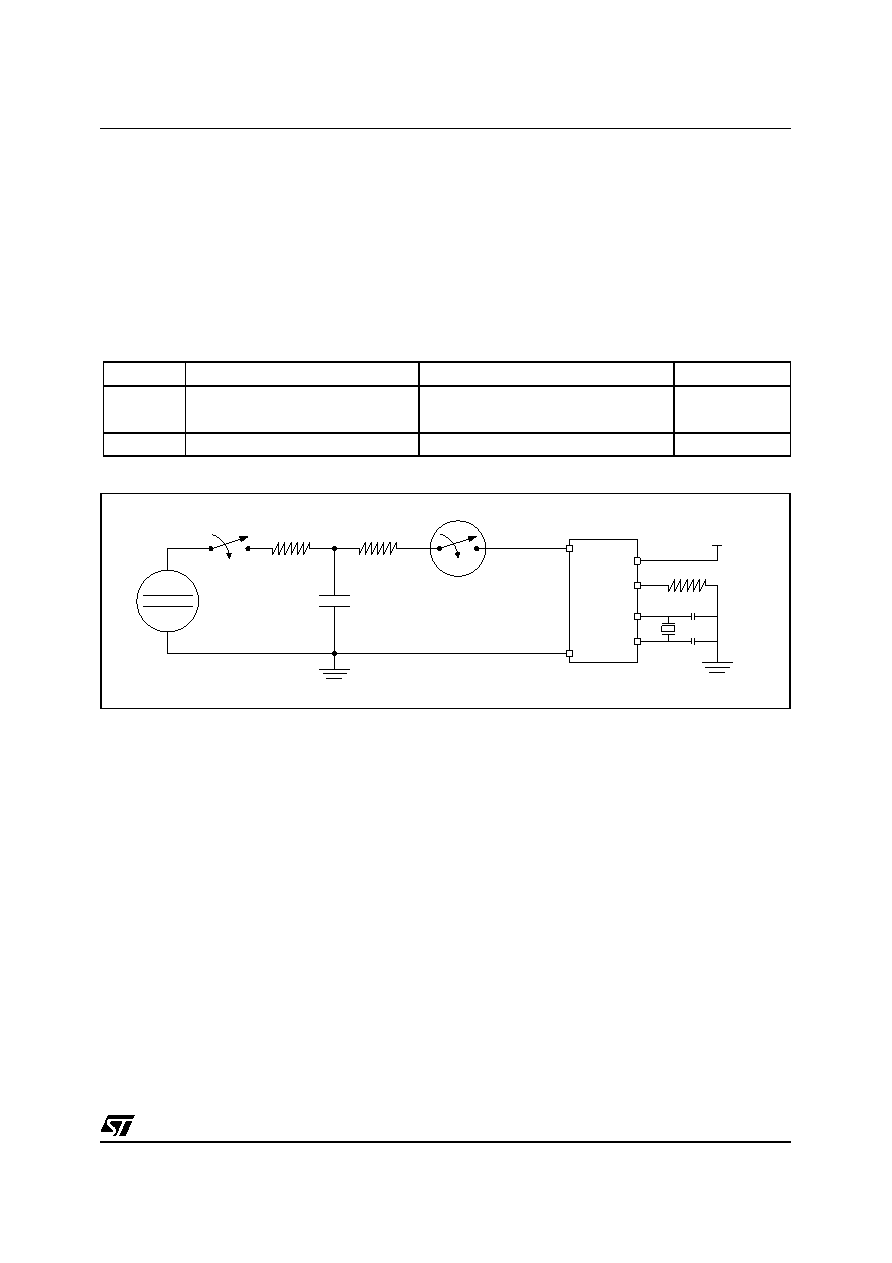
standards and is described in Figure 16.10.
Figure 16.10 Simplified Diagram of the ESD Generator for DLU
Notes:
1. Class description: Class A is an STMicroelectronics internal specification. All its limits are higher than
the JEDEC specification, that means when a device belongs to Class A it exceeds the JEDEC standard.
Class B strictly covers all the JEDEC criteria (international standard).
16.12.5 ESD Pin Protection Strategy. In order
to protect an integrated circuit against Electro-
Static Discharge the stress must be controlled to
prevent degradation or destruction of the circuit
elements. Stress generally affects the circuit
elements, which are connected to the pads but can
also affect the internal devices when the supply
pads receive the stress. The elements that are to
be protected must not receive excessive current,
voltage, or heating within their structure.
An ESD network combines the different input and
output protections. This network works by allowing
safe discharge paths for the pins subject to ESD
stress. Two critical ESD stress cases are
presented in Figure 16.11 and Figure 16.12 for
standard pins.
Standard Pin Protection
In order to protect the output structure the following
elements are added:
- A diode to VDD (3a) and a diode from VSS (3b)
- A protection device between VDD and VSS (4)
In order protect the input structure the following
elements are added:
- A resistor in series with pad (1)
- A diode to VDD (2a) and a diode from VSS (2b)
- A protection device between VDD and VSS (4)
Symbol
Parameter
Conditions
Class 1)
LU
Static latch-up class
TA=25° C
TA=85° C
A
DLU
Dynamic latch-up class
VDD=5.5V, fOSC= 8 MHz, TA=25° C
A
ST FIVE
V
DD
V
SS
DISCHARGE TIP
HV RELAY
DISCHARGE
RETURN CONNECTION
ESD
GENERATOR
R
D= 330 Ω
R
CH= 50 MΩ
C
S= 150 pF
相关PDF资料 |
PDF描述 |
|---|---|
| ST52E430B/D | 8-BIT, UVPROM, 20 MHz, MICROCONTROLLER, CDIP32 |
| ST52F510F1M6 | 8-BIT, FLASH, 24 MHz, MICROCONTROLLER, PDSO20 |
| ST52F510G0B6 | 8-BIT, FLASH, 24 MHz, MICROCONTROLLER, PDIP28 |
| ST52F513F0M6 | 8-BIT, FLASH, 24 MHz, MICROCONTROLLER, PDSO20 |
| ST52F513F1B6 | 8-BIT, FLASH, 24 MHz, MICROCONTROLLER, PDIP20 |
相关代理商/技术参数 |
参数描述 |
|---|---|
| ST52510G2 | 制造商:未知厂家 制造商全称:未知厂家 功能描述:8-BIT ICU WITH 10-BIT ADC. TWO TIMERS/PWM. I2C. SPI. SCI. UP TO 8K FLASH |
| ST52510G3 | 制造商:未知厂家 制造商全称:未知厂家 功能描述:8-BIT ICU WITH 10-BIT ADC. TWO TIMERS/PWM. I2C. SPI. SCI. UP TO 8K FLASH |
| ST52510K2 | 制造商:未知厂家 制造商全称:未知厂家 功能描述:8-BIT ICU WITH 10-BIT ADC. TWO TIMERS/PWM. I2C. SPI. SCI. UP TO 8K FLASH |
| ST52510K3 | 制造商:未知厂家 制造商全称:未知厂家 功能描述:8-BIT ICU WITH 10-BIT ADC. TWO TIMERS/PWM. I2C. SPI. SCI. UP TO 8K FLASH |
| ST52510Y2 | 制造商:未知厂家 制造商全称:未知厂家 功能描述:8-BIT ICU WITH 10-BIT ADC. TWO TIMERS/PWM. I2C. SPI. SCI. UP TO 8K FLASH |
发布紧急采购,3分钟左右您将得到回复。