- 您现在的位置:买卖IC网 > PDF目录98143 > ST52510F3M6 (STMICROELECTRONICS) MICROCONTROLLER, PDSO20 PDF资料下载
参数资料
| 型号: | ST52510F3M6 |
| 厂商: | STMICROELECTRONICS |
| 元件分类: | 微控制器/微处理器 |
| 英文描述: | MICROCONTROLLER, PDSO20 |
| 封装: | SOP-20 |
| 文件页数: | 135/136页 |
| 文件大小: | 3335K |
| 代理商: | ST52510F3M6 |
第1页第2页第3页第4页第5页第6页第7页第8页第9页第10页第11页第12页第13页第14页第15页第16页第17页第18页第19页第20页第21页第22页第23页第24页第25页第26页第27页第28页第29页第30页第31页第32页第33页第34页第35页第36页第37页第38页第39页第40页第41页第42页第43页第44页第45页第46页第47页第48页第49页第50页第51页第52页第53页第54页第55页第56页第57页第58页第59页第60页第61页第62页第63页第64页第65页第66页第67页第68页第69页第70页第71页第72页第73页第74页第75页第76页第77页第78页第79页第80页第81页第82页第83页第84页第85页第86页第87页第88页第89页第90页第91页第92页第93页第94页第95页第96页第97页第98页第99页第100页第101页第102页第103页第104页第105页第106页第107页第108页第109页第110页第111页第112页第113页第114页第115页第116页第117页第118页第119页第120页第121页第122页第123页第124页第125页第126页第127页第128页第129页第130页第131页第132页第133页第134页当前第135页第136页
Obsolete
Product(s)
- Obsolete
Product(s)
15 SERIAL PERIPHERAL INTERFACE (SPI)
15.1 Introduction
The Serial Peripheral Interface (SPI) allows full-
duplex, synchronous, serial communication with
external devices. An SPI system may consist of a
master, one or more slaves, or a system, in which
devices may be either masters or slaves.
SPI is normally used for communication between
the ICU and external peripherals or another ICU.
Refer to the Pin Description section in this
datasheet for the device-specific pin-out.
15.2 Main Features
■ Full duplex, three-wire synchronous transfers
■ Master or slave operation
■ Four master mode frequencies
■ Maximum slave mode frequency = fCKM/4.
■ Four programmable master bit rates
■ Programmable clock polarity and phase
■ End of transfer interrupt flag
■ Write collision flag protection
■ Master mode fault protection capability.
15.3 General description
SPI is connected to external devices through 4
alternate pins:
– MISO: Master In / Slave Out pin
– MOSI: Master Out / Slave In pin
– SCK: Serial Clock pin
–SS: Slave select pin (if not done through soft-
ware)
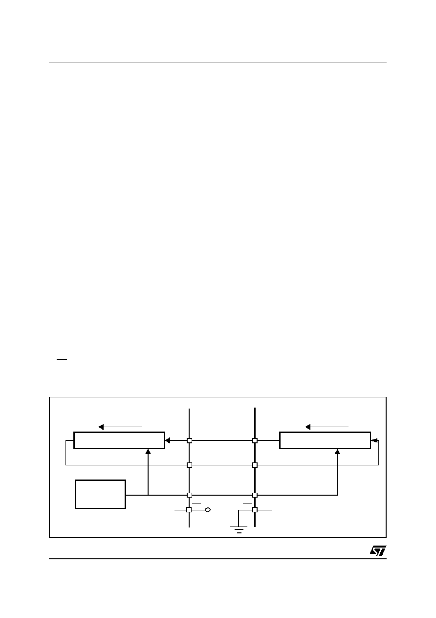
Figure 15.1 SPI Master Slave
A basic example of interconnections between a
single master and a single slave is illustrated in
The MOSI pins are connected together as the
MISO pins. In this manner, data is transferred
serially between master and slave (most significant
bit first).
When the master device transmits data to a slave
device via the MOSI pin, the slave device responds
by sending data to the master device via the MISO
pin. This implies full duplex transmission with both
data out and data in synchronized with the same
clock signal (which is provided by the master
device via the SCK pin).
The transmitted byte is replaced by the byte
received and eliminates the need for separate
transmit-empty and receiver-full bits. A status flag
is used to indicate that the I/O operation is
complete.
Four possible data/clock timing relationships may
be chosen (see Figure 15.4), but master and slave
must be programmed with the same timing mode.
15.4 Functional Description
Figure 15.2 shows the serial peripheral interface
(SPI) block diagram.
This interface contains 4 dedicated registers:
– A Control Register (SPI_CR)
– A Status Register (SPI_STATUS_CR)
– A Data Register for transmission (SPI_OUT)
– A Data Register for reception (SPI_IN)
15.4.1 Master Configuration.
In a master configuration, the serial clock is
generated on the SCK pin.
8-BIT SHIFT REGISTER
SPI
CLOCK
GENERATOR
8-BIT SHIFT REGISTER
MISO
MOSI
MISO
SCK
SLAVE
MASTER
SS
+5V
MSBit
LSBit
MSBit
LSBit
相关PDF资料 |
PDF描述 |
|---|---|
| ST52E430B/D | 8-BIT, UVPROM, 20 MHz, MICROCONTROLLER, CDIP32 |
| ST52F510F1M6 | 8-BIT, FLASH, 24 MHz, MICROCONTROLLER, PDSO20 |
| ST52F510G0B6 | 8-BIT, FLASH, 24 MHz, MICROCONTROLLER, PDIP28 |
| ST52F513F0M6 | 8-BIT, FLASH, 24 MHz, MICROCONTROLLER, PDSO20 |
| ST52F513F1B6 | 8-BIT, FLASH, 24 MHz, MICROCONTROLLER, PDIP20 |
相关代理商/技术参数 |
参数描述 |
|---|---|
| ST52510G2 | 制造商:未知厂家 制造商全称:未知厂家 功能描述:8-BIT ICU WITH 10-BIT ADC. TWO TIMERS/PWM. I2C. SPI. SCI. UP TO 8K FLASH |
| ST52510G3 | 制造商:未知厂家 制造商全称:未知厂家 功能描述:8-BIT ICU WITH 10-BIT ADC. TWO TIMERS/PWM. I2C. SPI. SCI. UP TO 8K FLASH |
| ST52510K2 | 制造商:未知厂家 制造商全称:未知厂家 功能描述:8-BIT ICU WITH 10-BIT ADC. TWO TIMERS/PWM. I2C. SPI. SCI. UP TO 8K FLASH |
| ST52510K3 | 制造商:未知厂家 制造商全称:未知厂家 功能描述:8-BIT ICU WITH 10-BIT ADC. TWO TIMERS/PWM. I2C. SPI. SCI. UP TO 8K FLASH |
| ST52510Y2 | 制造商:未知厂家 制造商全称:未知厂家 功能描述:8-BIT ICU WITH 10-BIT ADC. TWO TIMERS/PWM. I2C. SPI. SCI. UP TO 8K FLASH |
发布紧急采购,3分钟左右您将得到回复。