- 您现在的位置:买卖IC网 > PDF目录271212 > ST72F324BK6TATRE (STMICROELECTRONICS) 8-BIT, FLASH, 8 MHz, MICROCONTROLLER, PQFP32 PDF资料下载
参数资料
| 型号: | ST72F324BK6TATRE |
| 厂商: | STMICROELECTRONICS |
| 元件分类: | 微控制器/微处理器 |
| 英文描述: | 8-BIT, FLASH, 8 MHz, MICROCONTROLLER, PQFP32 |
| 封装: | 7 X 7 MM, ROHS COMPLIANT, LQFP-32 |
| 文件页数: | 119/197页 |
| 文件大小: | 3593K |
| 代理商: | ST72F324BK6TATRE |
第1页第2页第3页第4页第5页第6页第7页第8页第9页第10页第11页第12页第13页第14页第15页第16页第17页第18页第19页第20页第21页第22页第23页第24页第25页第26页第27页第28页第29页第30页第31页第32页第33页第34页第35页第36页第37页第38页第39页第40页第41页第42页第43页第44页第45页第46页第47页第48页第49页第50页第51页第52页第53页第54页第55页第56页第57页第58页第59页第60页第61页第62页第63页第64页第65页第66页第67页第68页第69页第70页第71页第72页第73页第74页第75页第76页第77页第78页第79页第80页第81页第82页第83页第84页第85页第86页第87页第88页第89页第90页第91页第92页第93页第94页第95页第96页第97页第98页第99页第100页第101页第102页第103页第104页第105页第106页第107页第108页第109页第110页第111页第112页第113页第114页第115页第116页第117页第118页当前第119页第120页第121页第122页第123页第124页第125页第126页第127页第128页第129页第130页第131页第132页第133页第134页第135页第136页第137页第138页第139页第140页第141页第142页第143页第144页第145页第146页第147页第148页第149页第150页第151页第152页第153页第154页第155页第156页第157页第158页第159页第160页第161页第162页第163页第164页第165页第166页第167页第168页第169页第170页第171页第172页第173页第174页第175页第176页第177页第178页第179页第180页第181页第182页第183页第184页第185页第186页第187页第188页第189页第190页第191页第192页第193页第194页第195页第196页第197页
Obsolete
Product(s)
- Obsolete
Product(s)
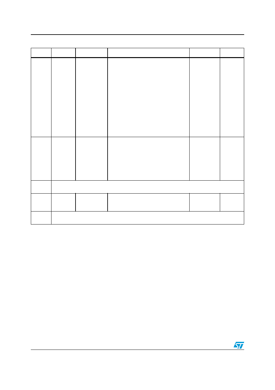
Register and memory map
ST72324B-Auto
Legend: x = undefined, R/W = read/write
0041h
0042h
0043h
0044h
0045h
0046h
0047h
0048h
0049h
004Ah
004Bh
004Ch
004Dh
004Eh
004Fh
Timer B
TBCR2
TBCR1
TBCSR
TBIC1HR
TBIC1LR
TBOC1HR
TBOC1LR
TBCHR
TBCLR
TBACHR
TBACLR
TBIC2HR
TBIC2LR
TBOC2HR
TBOC2LR
Timer B control register 2
Timer B control register 1
Timer B control/status register
Timer B input capture 1 high register
Timer B input capture 1 low register
Timer B output compare 1 high register
Timer B output compare 1 low register
Timer B counter high register
Timer B counter low register
Timer B alternate counter high register
Timer B alternate counter low register
Timer B input capture 2 high register
Timer B input capture 2 low register
Timer B output compare 2 high register
Timer B output compare 2 low register
00h
xxxx x0xxb
xxh
80h
00h
FFh
FCh
FFh
FCh
xxh
80h
00h
R/W
Read only
R/W
Read only
R/W
0050h
0051h
0052h
0053h
0054h
0055h
0056h
0057h
SCI
SCISR
SCIDR
SCIBRR
SCICR1
SCICR2
SCIERPR
SCIETPR
SCI status register
SCI data register
SCI baud rate register
SCI control register 1
SCI control register 2
SCI extended receive prescaler register
Reserved area
SCI extended transmit prescaler register
C0h
xxh
00h
x000 0000b
00h
---
00h
Read only
R/W
0058h to
006Fh
Reserved area (24 bytes)
0070h
0071h
0072h
ADC
ADCCSR
ADCDRH
ADCDRL
Control/status register
Data high register
Data low register
00h
R/W
Read only
0073h
007Fh
Reserved area (13 bytes)
1.
The bits associated with unavailable pins must always keep their reset value.
2.
The contents of the I/O port DR registers are readable only in output configuration. In input configuration, the values of the
I/O pins are returned instead of the DR register contents.
Table 3.
Hardware register map (continued)
Address
Block
Register label
Register name
Reset status
Remarks
相关PDF资料 |
PDF描述 |
|---|---|
| SAB-C161K-LMHA | 16-BIT, 20 MHz, MICROCONTROLLER, PQFP80 |
| ST72P561R4TA/XXX | 8-BIT, MROM, 8 MHz, MICROCONTROLLER, PQFP64 |
| ST7263BH4T1/XXX | 8-BIT, MROM, 8 MHz, MICROCONTROLLER, PQFP48 |
| S912XDT384J1VAGR | 16-BIT, FLASH, 40 MHz, MICROCONTROLLER, PQFP144 |
| SC101161DGCFUR2 | 16-BIT, FLASH, 25 MHz, MICROCONTROLLER, PQFP80 |
相关代理商/技术参数 |
参数描述 |
|---|---|
| ST72F324BK6TAXS | 制造商:STMicroelectronics 功能描述: |
| ST72F324BK6TCE | 制造商:STMicroelectronics 功能描述: |
| ST72F324BK6TCS | 制造商:STMicroelectronics 功能描述:APG |
| ST72F324BK6TCTRE | 制造商:STMicroelectronics 功能描述:LQFP 32 7x7x1.4 1 |
| ST72F324J2B6 | 制造商:STMicroelectronics 功能描述: |
发布紧急采购,3分钟左右您将得到回复。