- 您现在的位置:买卖IC网 > PDF目录271212 > ST72F324BK6TATRE (STMICROELECTRONICS) 8-BIT, FLASH, 8 MHz, MICROCONTROLLER, PQFP32 PDF资料下载
参数资料
| 型号: | ST72F324BK6TATRE |
| 厂商: | STMICROELECTRONICS |
| 元件分类: | 微控制器/微处理器 |
| 英文描述: | 8-BIT, FLASH, 8 MHz, MICROCONTROLLER, PQFP32 |
| 封装: | 7 X 7 MM, ROHS COMPLIANT, LQFP-32 |
| 文件页数: | 84/197页 |
| 文件大小: | 3593K |
| 代理商: | ST72F324BK6TATRE |
第1页第2页第3页第4页第5页第6页第7页第8页第9页第10页第11页第12页第13页第14页第15页第16页第17页第18页第19页第20页第21页第22页第23页第24页第25页第26页第27页第28页第29页第30页第31页第32页第33页第34页第35页第36页第37页第38页第39页第40页第41页第42页第43页第44页第45页第46页第47页第48页第49页第50页第51页第52页第53页第54页第55页第56页第57页第58页第59页第60页第61页第62页第63页第64页第65页第66页第67页第68页第69页第70页第71页第72页第73页第74页第75页第76页第77页第78页第79页第80页第81页第82页第83页当前第84页第85页第86页第87页第88页第89页第90页第91页第92页第93页第94页第95页第96页第97页第98页第99页第100页第101页第102页第103页第104页第105页第106页第107页第108页第109页第110页第111页第112页第113页第114页第115页第116页第117页第118页第119页第120页第121页第122页第123页第124页第125页第126页第127页第128页第129页第130页第131页第132页第133页第134页第135页第136页第137页第138页第139页第140页第141页第142页第143页第144页第145页第146页第147页第148页第149页第150页第151页第152页第153页第154页第155页第156页第157页第158页第159页第160页第161页第162页第163页第164页第165页第166页第167页第168页第169页第170页第171页第172页第173页第174页第175页第176页第177页第178页第179页第180页第181页第182页第183页第184页第185页第186页第187页第188页第189页第190页第191页第192页第193页第194页第195页第196页第197页
Obsolete
Product(s)
- Obsolete
Product(s)
Electrical characteristics
ST72324B-Auto
174/197
12.13.1
Analog power supply and reference pins
Depending on the MCU pin count, the package may feature separate VAREF and VSSA
analog power supply pins. These pins supply power to the A/D converter cell and function
as the high and low reference voltages for the conversion. In some packages, VAREF and
and reference pads are internally bonded to the VDD and VSS pins.
Separation of the digital and analog power pins allow board designers to improve A/D
performance. Conversion accuracy can be impacted by voltage drops and noise in the event
of heavily loaded or badly decoupled power supply lines (see Section 12.13.2: General PCB
12.13.2
General PCB design guidelines
To obtain best results, some general design and layout rules should be followed when
designing the application PCB to shield the noise-sensitive, analog physical interface from
noise-generating CMOS logic signals.
●
Use separate digital and analog planes. The analog ground plane should be connected
to the digital ground plane via a single point on the PCB.
●
Filter power to the analog power planes. It is recommended to connect capacitors, with
good high frequency characteristics, between the power and ground lines, placing
0.1F and optionally, if needed 10pF capacitors as close as possible to the ST7 power
supply pins and a 1 to 10F capacitor close to the power source (see Figure 85).
●
The analog and digital power supplies should be connected in a star network. Do not
use a resistor, as VAREF is used as a reference voltage by the A/D converter and any
resistance would cause a voltage drop and a loss of accuracy.
●
Properly place components and route the signal traces on the PCB to shield the analog
inputs. Analog signals paths should run over the analog ground plane and be as short
as possible. Isolate analog signals from digital signals that may switch while the analog
inputs are being sampled by the A/D converter. Do not toggle digital outputs on the
same I/O port as the A/D input being converted.
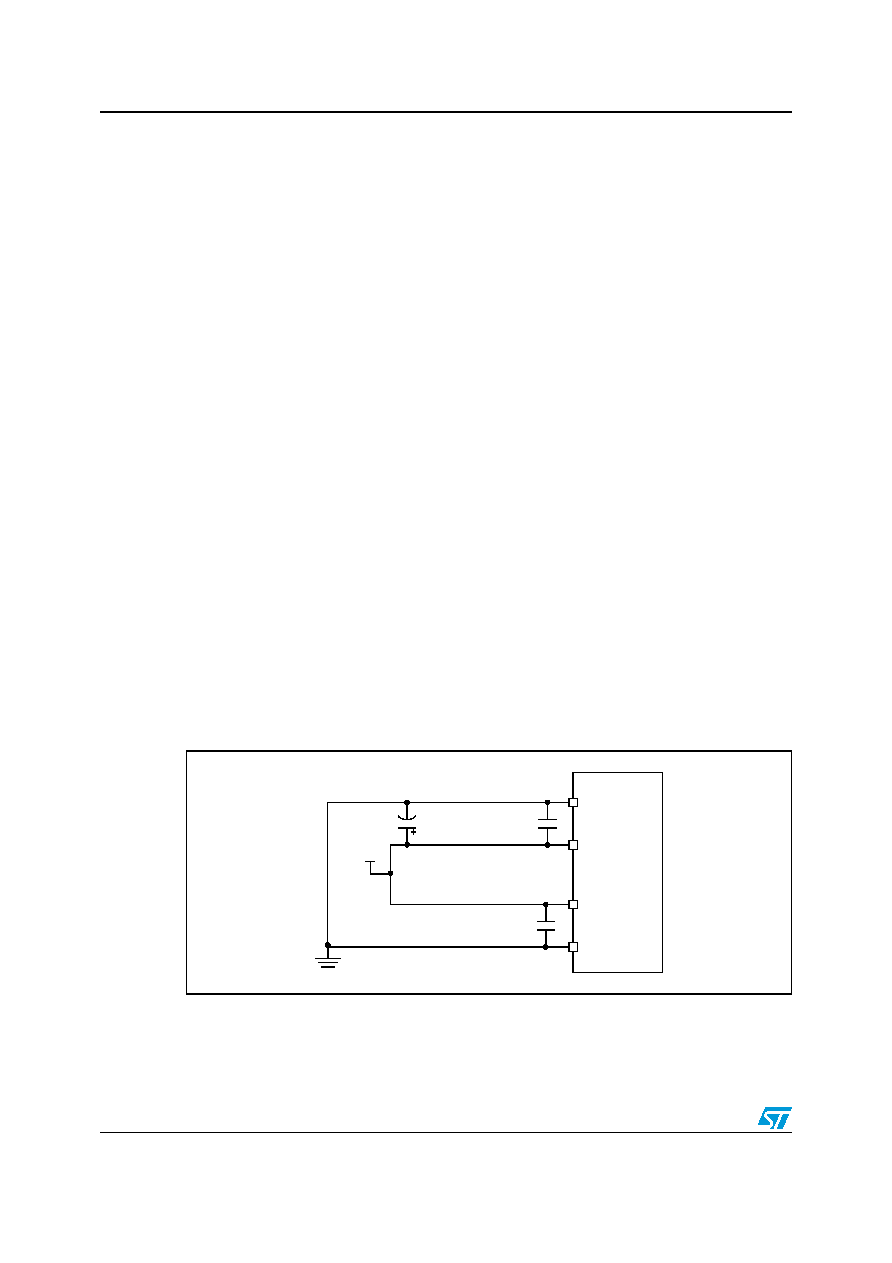
Figure 85.
Power supply filtering
VSS
VDD
ST72XXX
VAREF
VSSA
Power
supply
source
ST7
digital noise
filtering
External
noise
filtering
1 to 10F
0.1F
相关PDF资料 |
PDF描述 |
|---|---|
| SAB-C161K-LMHA | 16-BIT, 20 MHz, MICROCONTROLLER, PQFP80 |
| ST72P561R4TA/XXX | 8-BIT, MROM, 8 MHz, MICROCONTROLLER, PQFP64 |
| ST7263BH4T1/XXX | 8-BIT, MROM, 8 MHz, MICROCONTROLLER, PQFP48 |
| S912XDT384J1VAGR | 16-BIT, FLASH, 40 MHz, MICROCONTROLLER, PQFP144 |
| SC101161DGCFUR2 | 16-BIT, FLASH, 25 MHz, MICROCONTROLLER, PQFP80 |
相关代理商/技术参数 |
参数描述 |
|---|---|
| ST72F324BK6TAXS | 制造商:STMicroelectronics 功能描述: |
| ST72F324BK6TCE | 制造商:STMicroelectronics 功能描述: |
| ST72F324BK6TCS | 制造商:STMicroelectronics 功能描述:APG |
| ST72F324BK6TCTRE | 制造商:STMicroelectronics 功能描述:LQFP 32 7x7x1.4 1 |
| ST72F324J2B6 | 制造商:STMicroelectronics 功能描述: |
发布紧急采购,3分钟左右您将得到回复。