- 您现在的位置:买卖IC网 > PDF目录271212 > ST72F324BK6TATRE (STMICROELECTRONICS) 8-BIT, FLASH, 8 MHz, MICROCONTROLLER, PQFP32 PDF资料下载
参数资料
| 型号: | ST72F324BK6TATRE |
| 厂商: | STMICROELECTRONICS |
| 元件分类: | 微控制器/微处理器 |
| 英文描述: | 8-BIT, FLASH, 8 MHz, MICROCONTROLLER, PQFP32 |
| 封装: | 7 X 7 MM, ROHS COMPLIANT, LQFP-32 |
| 文件页数: | 91/197页 |
| 文件大小: | 3593K |
| 代理商: | ST72F324BK6TATRE |
第1页第2页第3页第4页第5页第6页第7页第8页第9页第10页第11页第12页第13页第14页第15页第16页第17页第18页第19页第20页第21页第22页第23页第24页第25页第26页第27页第28页第29页第30页第31页第32页第33页第34页第35页第36页第37页第38页第39页第40页第41页第42页第43页第44页第45页第46页第47页第48页第49页第50页第51页第52页第53页第54页第55页第56页第57页第58页第59页第60页第61页第62页第63页第64页第65页第66页第67页第68页第69页第70页第71页第72页第73页第74页第75页第76页第77页第78页第79页第80页第81页第82页第83页第84页第85页第86页第87页第88页第89页第90页当前第91页第92页第93页第94页第95页第96页第97页第98页第99页第100页第101页第102页第103页第104页第105页第106页第107页第108页第109页第110页第111页第112页第113页第114页第115页第116页第117页第118页第119页第120页第121页第122页第123页第124页第125页第126页第127页第128页第129页第130页第131页第132页第133页第134页第135页第136页第137页第138页第139页第140页第141页第142页第143页第144页第145页第146页第147页第148页第149页第150页第151页第152页第153页第154页第155页第156页第157页第158页第159页第160页第161页第162页第163页第164页第165页第166页第167页第168页第169页第170页第171页第172页第173页第174页第175页第176页第177页第178页第179页第180页第181页第182页第183页第184页第185页第186页第187页第188页第189页第190页第191页第192页第193页第194页第195页第196页第197页
Obsolete
Product(s)
- Obsolete
Product(s)
Device configuration and ordering information
ST72324B-Auto
180/197
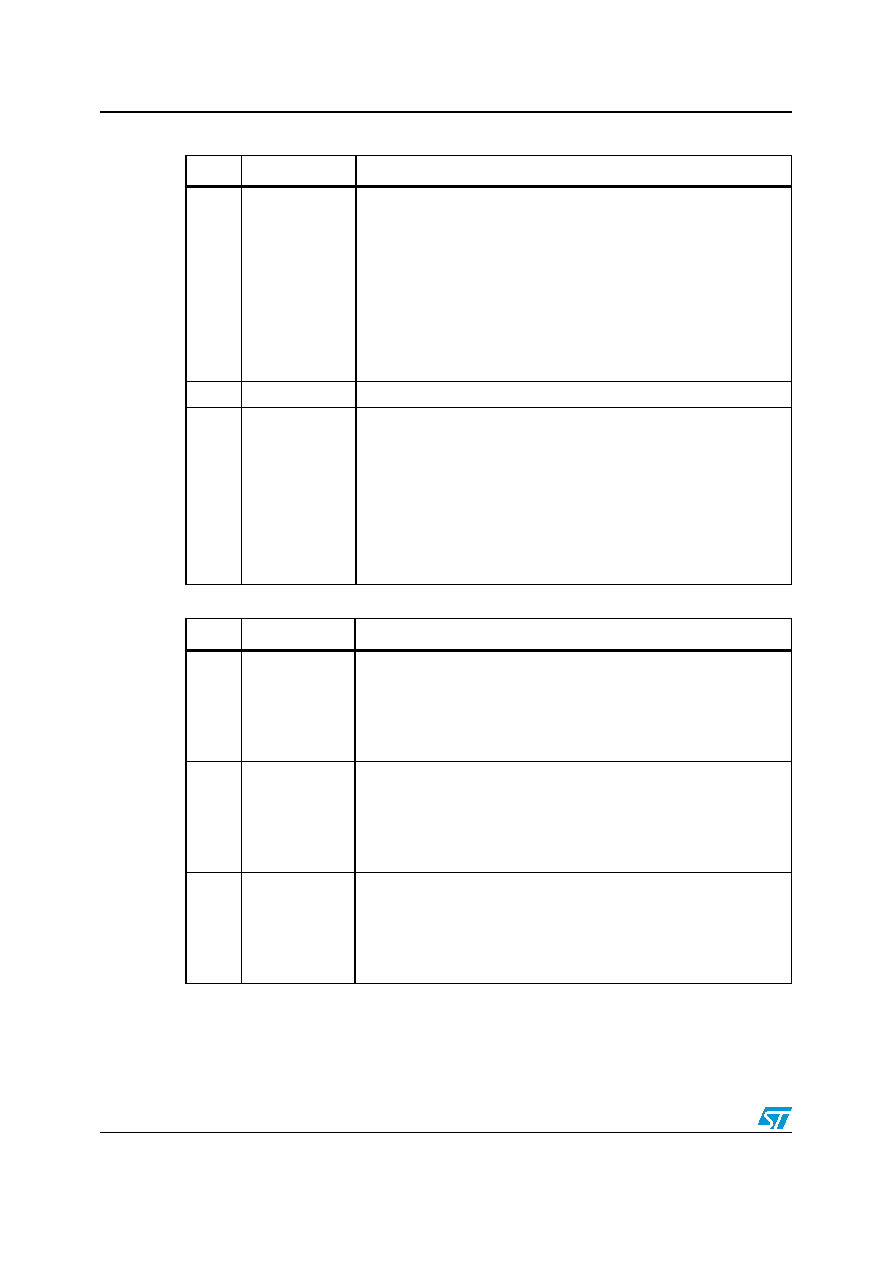
OPT4:3
VD[1:0]
Voltage detection
These option bits enable the voltage detection block (LVD and AVD)
with a selected threshold for the LVD and AVD.
00: Selected LVD = Highest threshold (VDD~4V).
01: Selected LVD = Medium threshold (VDD~3.5V).
10: Selected LVD = Lowest threshold (VDD~3V).
11: LVD and AVD off
Caution: If the medium or low thresholds are selected, the detection
may occur outside the specified operating voltage range. Below 3.8V,
device operation is not guaranteed. For details on the AVD and LVD
threshold levels refer to Section 12.4.1 on page 151.
OPT2:1
-
Reserved, must be kept at default value
OPT0
FMP_R
Flash memory readout protection
Readout protection, when selected, provides a protection against
program memory content extraction and against write access to Flash
memory.
Erasing the option bytes when the FMP_R option is selected causes
the whole user memory to be erased first, afterwhich the device can
be reprogrammed. Refer to Section 4.3.1 on page 30 and the ST7
Flash Programming Reference Manual for more details.
0: Readout protection enabled
1: Readout protection disabled
Table 119.
Option byte 1 bit description
Bit
Name
Function
OPT7
PKG1
Pin package selection bit
This option bit selects the package (see Table 120).
Note: On the chip, each I/O port has eight pads. Pads that are not
bonded to external pins are in input pull-up configuration after reset.
The configuration of these pads must be kept at reset state to avoid
added current consumption.
OPT6
RSTC
Reset clock cycle selection
This option bit selects the number of CPU cycles applied during the
reset phase and when exiting Halt mode. For resonator oscillators, it
is advised to select 4096 due to the long crystal stabilization time.
0: Reset phase with 4096 CPU cycles
1: Reset phase with 256 CPU cycles
OPT5:4
OSCTYPE[1:0]
Oscillator type
These option bits select the ST7 main clock source type.
00: Clock source = Resonator oscillator
01: Reserved
10: Clock source = Internal RC oscillator
11: Clock source = External source
Table 118.
Option byte 0 bit description (continued)
Bit
Name
Function
相关PDF资料 |
PDF描述 |
|---|---|
| SAB-C161K-LMHA | 16-BIT, 20 MHz, MICROCONTROLLER, PQFP80 |
| ST72P561R4TA/XXX | 8-BIT, MROM, 8 MHz, MICROCONTROLLER, PQFP64 |
| ST7263BH4T1/XXX | 8-BIT, MROM, 8 MHz, MICROCONTROLLER, PQFP48 |
| S912XDT384J1VAGR | 16-BIT, FLASH, 40 MHz, MICROCONTROLLER, PQFP144 |
| SC101161DGCFUR2 | 16-BIT, FLASH, 25 MHz, MICROCONTROLLER, PQFP80 |
相关代理商/技术参数 |
参数描述 |
|---|---|
| ST72F324BK6TAXS | 制造商:STMicroelectronics 功能描述: |
| ST72F324BK6TCE | 制造商:STMicroelectronics 功能描述: |
| ST72F324BK6TCS | 制造商:STMicroelectronics 功能描述:APG |
| ST72F324BK6TCTRE | 制造商:STMicroelectronics 功能描述:LQFP 32 7x7x1.4 1 |
| ST72F324J2B6 | 制造商:STMicroelectronics 功能描述: |
发布紧急采购,3分钟左右您将得到回复。