- 您现在的位置:买卖IC网 > PDF目录271212 > ST72F324BK6TATRE (STMICROELECTRONICS) 8-BIT, FLASH, 8 MHz, MICROCONTROLLER, PQFP32 PDF资料下载
参数资料
| 型号: | ST72F324BK6TATRE |
| 厂商: | STMICROELECTRONICS |
| 元件分类: | 微控制器/微处理器 |
| 英文描述: | 8-BIT, FLASH, 8 MHz, MICROCONTROLLER, PQFP32 |
| 封装: | 7 X 7 MM, ROHS COMPLIANT, LQFP-32 |
| 文件页数: | 195/197页 |
| 文件大小: | 3593K |
| 代理商: | ST72F324BK6TATRE |
第1页第2页第3页第4页第5页第6页第7页第8页第9页第10页第11页第12页第13页第14页第15页第16页第17页第18页第19页第20页第21页第22页第23页第24页第25页第26页第27页第28页第29页第30页第31页第32页第33页第34页第35页第36页第37页第38页第39页第40页第41页第42页第43页第44页第45页第46页第47页第48页第49页第50页第51页第52页第53页第54页第55页第56页第57页第58页第59页第60页第61页第62页第63页第64页第65页第66页第67页第68页第69页第70页第71页第72页第73页第74页第75页第76页第77页第78页第79页第80页第81页第82页第83页第84页第85页第86页第87页第88页第89页第90页第91页第92页第93页第94页第95页第96页第97页第98页第99页第100页第101页第102页第103页第104页第105页第106页第107页第108页第109页第110页第111页第112页第113页第114页第115页第116页第117页第118页第119页第120页第121页第122页第123页第124页第125页第126页第127页第128页第129页第130页第131页第132页第133页第134页第135页第136页第137页第138页第139页第140页第141页第142页第143页第144页第145页第146页第147页第148页第149页第150页第151页第152页第153页第154页第155页第156页第157页第158页第159页第160页第161页第162页第163页第164页第165页第166页第167页第168页第169页第170页第171页第172页第173页第174页第175页第176页第177页第178页第179页第180页第181页第182页第183页第184页第185页第186页第187页第188页第189页第190页第191页第192页第193页第194页当前第195页第196页第197页
Obsolete
Product(s)
- Obsolete
Product(s)
ST72324B-Auto
On-chip peripherals
97/197
Control/Status Register (CSR)
M
5OPM
One Pulse Mode
0: One Pulse mode is not active.
1: One Pulse mode is active, the ICAP1 pin can be used to trigger one pulse on the
OCMP1 pin; the active transition is given by the IEDG1 bit. The length of the
generated pulse depends on the contents of the OC1R register.
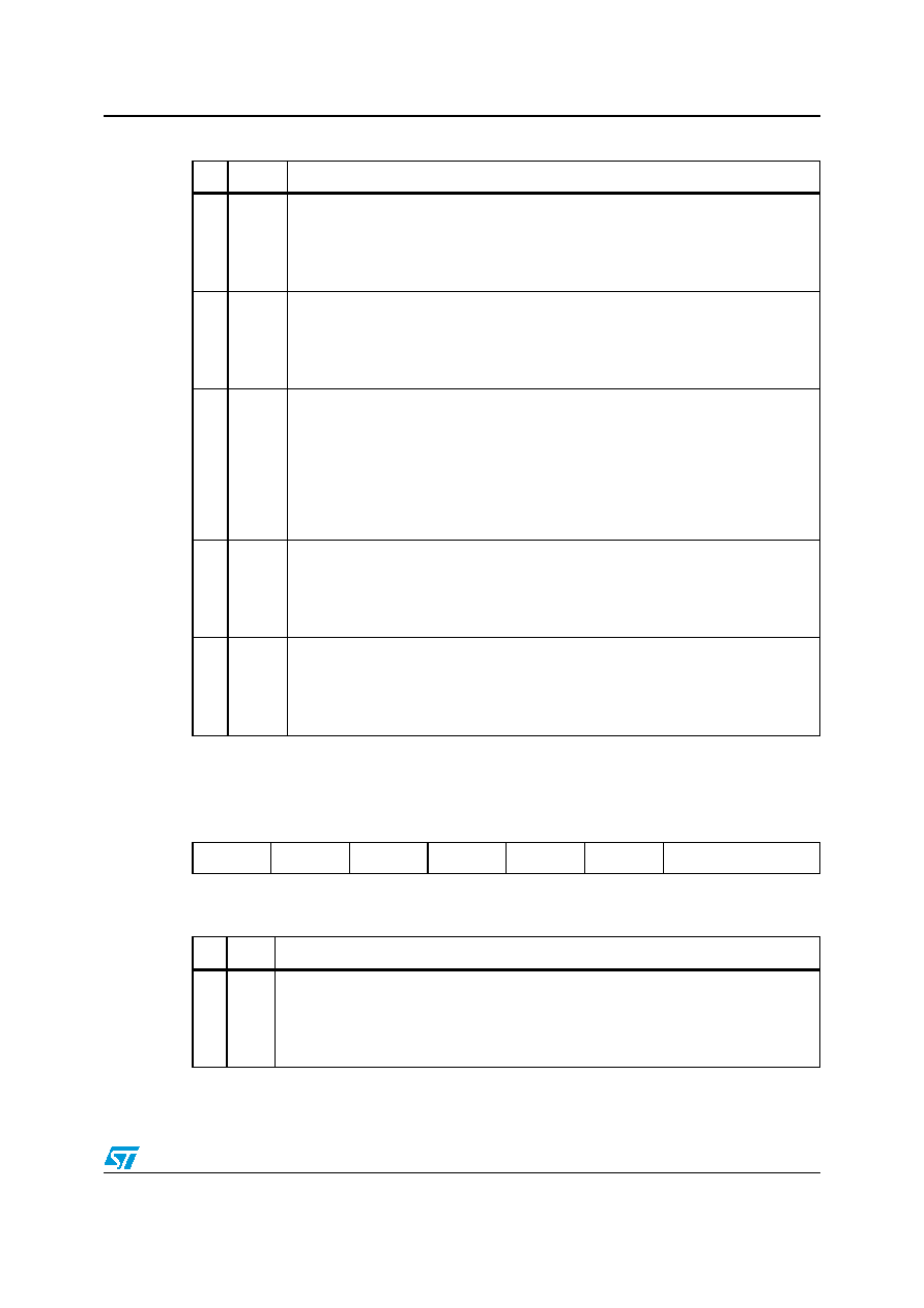
4PWM
Pulse Width Modulation
0: PWM mode is not active.
1: PWM mode is active, the OCMP1 pin outputs a programmable cyclic signal; the
length of the pulse depends on the value of OC1R register; the period depends on
the value of OC2R register.
3:2
CC[1:0]
Clock Control
The timer clock mode depends on these bits.
00: Timer clock = fCPU/4
01: Timer clock = fCPU/2
10: Timer clock = fCPU/8
11: Timer clock = external clock (where available)
Note: If the external clock pin is not available, programming the external clock
configuration stops the counter.
1IEDG2
Input Edge 2
This bit determines which type of level transition on the ICAP2 pin will trigger the
capture.
0: A falling edge triggers the capture.
1: A rising edge triggers the capture.
0
EXEDG
External Clock Edge
This bit determines which type of level transition on the external clock pin EXTCLK
will trigger the counter register.
0: A falling edge triggers the counter register.
1: A rising edge triggers the counter register.
CSR
Reset value: xxxx x0xx (xxh)
7
654
32
10
ICF1
OCF1
TOF
ICF2
OCF2
TIMD
Reserved
RO
R/W
-
Table 51.
CSR register description
Bit
Name
Function
7ICF1
Input Capture Flag 1
0: No Input Capture (reset value).
1: An Input Capture has occurred on the ICAP1 pin or the counter has reached the
OC2R value in PWM mode. To clear this bit, first read the SR register, then read or
write the low byte of the IC1R (IC1LR) register.
Table 50.
CR2 register description (continued)
Bit
Name
Function
相关PDF资料 |
PDF描述 |
|---|---|
| SAB-C161K-LMHA | 16-BIT, 20 MHz, MICROCONTROLLER, PQFP80 |
| ST72P561R4TA/XXX | 8-BIT, MROM, 8 MHz, MICROCONTROLLER, PQFP64 |
| ST7263BH4T1/XXX | 8-BIT, MROM, 8 MHz, MICROCONTROLLER, PQFP48 |
| S912XDT384J1VAGR | 16-BIT, FLASH, 40 MHz, MICROCONTROLLER, PQFP144 |
| SC101161DGCFUR2 | 16-BIT, FLASH, 25 MHz, MICROCONTROLLER, PQFP80 |
相关代理商/技术参数 |
参数描述 |
|---|---|
| ST72F324BK6TAXS | 制造商:STMicroelectronics 功能描述: |
| ST72F324BK6TCE | 制造商:STMicroelectronics 功能描述: |
| ST72F324BK6TCS | 制造商:STMicroelectronics 功能描述:APG |
| ST72F324BK6TCTRE | 制造商:STMicroelectronics 功能描述:LQFP 32 7x7x1.4 1 |
| ST72F324J2B6 | 制造商:STMicroelectronics 功能描述: |
发布紧急采购,3分钟左右您将得到回复。