- 您现在的位置:买卖IC网 > PDF目录385871 > ST72T85A5Q6 (意法半导体) 8-BIT MCU FOR RDS WITH 48K ROM, 3K RAM, ADC, TWO TIMERS, TWO SPIs, I2C AND SCI INTERFACES PDF资料下载
参数资料
| 型号: | ST72T85A5Q6 |
| 厂商: | 意法半导体 |
| 英文描述: | 8-BIT MCU FOR RDS WITH 48K ROM, 3K RAM, ADC, TWO TIMERS, TWO SPIs, I2C AND SCI INTERFACES |
| 中文描述: | 8位微控制器48,000铁路发展策略光盘,3K内存,ADC,两个定时器,2个SPI,I2C和脊髓损伤接口 |
| 文件页数: | 29/117页 |
| 文件大小: | 748K |
| 代理商: | ST72T85A5Q6 |
第1页第2页第3页第4页第5页第6页第7页第8页第9页第10页第11页第12页第13页第14页第15页第16页第17页第18页第19页第20页第21页第22页第23页第24页第25页第26页第27页第28页当前第29页第30页第31页第32页第33页第34页第35页第36页第37页第38页第39页第40页第41页第42页第43页第44页第45页第46页第47页第48页第49页第50页第51页第52页第53页第54页第55页第56页第57页第58页第59页第60页第61页第62页第63页第64页第65页第66页第67页第68页第69页第70页第71页第72页第73页第74页第75页第76页第77页第78页第79页第80页第81页第82页第83页第84页第85页第86页第87页第88页第89页第90页第91页第92页第93页第94页第95页第96页第97页第98页第99页第100页第101页第102页第103页第104页第105页第106页第107页第108页第109页第110页第111页第112页第113页第114页第115页第116页第117页
29/117
ST7285C
SERIAL COMMUNICATIONS INTERFACE
(Cont’d)
Each receiving device decodes this address head-
er under program control and all non addressed
receivers may be placed in a sleep mode by
means of the Muting function, thus avoiding the
message contents from generating unnecessary
requests for service. This is achieved by inhibiting
all reception flags and interrupt generation when
Muting is enabled. A muted receiver may be re-
awakened in one of two ways: by Idle Line detec-
tion or by Address Mark detection. The wake-up
method may be programmed by programming the
WAKE bit in the SCCR1 register.
Receiver wake-up by Idle Line detection takes
place as soon as the Receive line is recognised as
being idle. An Idle Line condition is detected upon
receiving 10 or 11 consecutive ”ones”, depending
on whether a word has been defined as compris-
ing 8 or 9 data bits. This wake-up method is select-
ed by programming the WAKE bit to ”0”.
Receiver wake-up by Address Mark detection
takes place on receiving a ”1” as the most signifi-
cant bit of a word, thus indicating that the message
is an address. This wake-up method is selected by
programming the WAKE bit to ”1”.
4.2.6 Baud Rate Generation
The following description is best read with refer-
ence to the SCI Baud Rate and External Prescaler
Diagram illustrated in Figure 2.
The CPU Clock is first divided by 16 by the first di-
visor block, then again divided by the division fac-
tor selected for the first prescaler, indicated by PR.
This division factor can be selected to be 1, 3, 4 or
13, depending on the setting of the SCP0 and
SCP1 bits (bits 6 and 7) in the SCBRR register (re-
fer to the register description). The output from the
first prescaler will thus be the CPU Clock frequen-
cy divided by 16, 48, 64 or 208. This master clock
is available both to the conventional Baud Rate
Generator and to the External Prescaler.
The conventional Baud Rate Generator is enabled
by setting the relevant section (RX or TX) of the
External Prescaler to 00h. In this case the master
clock frequency is further divided by 1, 2, 4, 8, 16,
32, 64 or 128, depending on the settings of bits
SCT0, SCT1 and SCT2 in the case of the transmit-
ter, and SCR0, SCR1 and SCR2 in the case of the
receiver (refer to the SCBRR register description).
If the External Prescaler Receive or Transmit
Baud Rate Register, PSBRT or PSBRR is set to a
value other than zero, that section of the prescaler
will be operational in place of the conventional
Baud Rate Generator. The output clock rate sent
to the transmitter or to the receiver will be the out-
put from the first prescaler divided by a factor
ranging from 1 to 255 set in the External Prescaler
Receive or Transmit Baud Rate Register. As can
be seen the External Prescaler option gives a very
fine degree of control on the Baud rate, whereas
the conventional Baud Rate Generator retains in-
dustry standard software compatibility.
4.2.7 SCI Register Overview
The registers described in the following para-
graphs allow full control of the various features
and parameters of the Serial Communications In-
terface. Refer also to the Memory Map.
4.2.7.1 Data Register (SCDR)
Address: 0051h
—
Read/Write
Reset Value: XXh
Contains the Received or Transmitted data char-
acter, depending on whether it is read or written to.
4.2.7.2 Control Register 1 (SCCR1)
Address: 0053h
—
Read/Write
Reset Value: XXh
Contains bits to selectthe desired word length and
the wake-up mode.
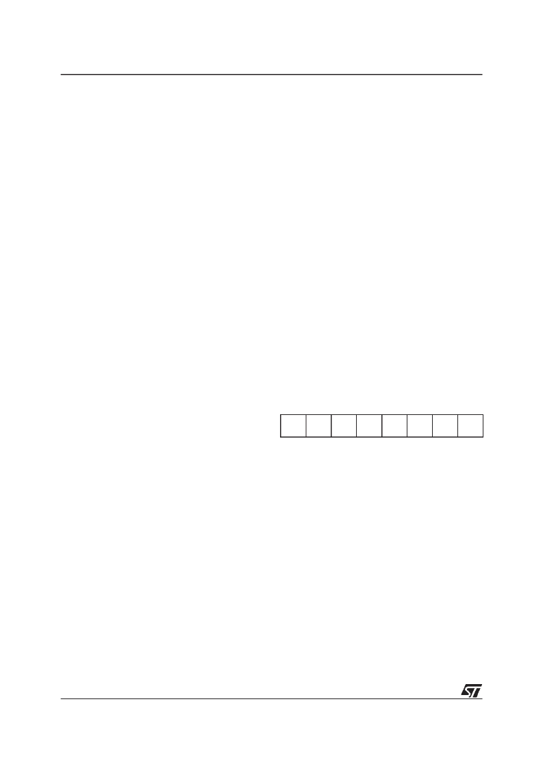
Bit-7 =
R8
Receive Data Bit 8
If bit M is set at one, R8 will be used to store the
9th bit on reception.
Bit-6 =
T8
Transmit Data Bit 8
Used to store the 9th data bit of the transmitted
word, when 9-bit word length is selected (bit M set
to ”1”).
Bit-4 =
M
Word Length
Determines the word length:
0 = 1 Start bit, 8 Data bits, 1 Stop bit
1 = 1 Start bit, 9 Data bits, 1 Stop bit
Bit-3 =
WAKE
Wake-Up Method
1 = Address Mark
0 = Idle Line
7
6
5
4
3
2
1
0
R8
T8
-
M
WAKE
-
-
-
相关PDF资料 |
PDF描述 |
|---|---|
| ST730C08L3 | PHASE CONTROL THYRISTORS |
| ST730C08L3L | PHASE CONTROL THYRISTORS |
| ST730C12L0 | PHASE CONTROL THYRISTORS |
| ST730C12L0L | PHASE CONTROL THYRISTORS |
| ST730C12L1 | PHASE CONTROL THYRISTORS |
相关代理商/技术参数 |
参数描述 |
|---|---|
| ST730 | 制造商:IRF 制造商全称:International Rectifier 功能描述:PHASE CONTROL THYRISTORS Hockey Puk Version |
| ST7-30 | 制造商:SUPERWORLD 制造商全称:Superworld Electronics 功能描述:POWER TRANSFORMER |
| ST-7300 | 制造商:GC Electronics 功能描述: |
| ST730186-3 | 制造商:KEMET Corporation 功能描述: 制造商:KET 功能描述: |
| ST730268-1 | 制造商:KEMET Corporation 功能描述: 制造商:KET 功能描述: |
发布紧急采购,3分钟左右您将得到回复。