- 您现在的位置:买卖IC网 > PDF目录385871 > ST72T85A5Q6 (意法半导体) 8-BIT MCU FOR RDS WITH 48K ROM, 3K RAM, ADC, TWO TIMERS, TWO SPIs, I2C AND SCI INTERFACES PDF资料下载
参数资料
| 型号: | ST72T85A5Q6 |
| 厂商: | 意法半导体 |
| 英文描述: | 8-BIT MCU FOR RDS WITH 48K ROM, 3K RAM, ADC, TWO TIMERS, TWO SPIs, I2C AND SCI INTERFACES |
| 中文描述: | 8位微控制器48,000铁路发展策略光盘,3K内存,ADC,两个定时器,2个SPI,I2C和脊髓损伤接口 |
| 文件页数: | 31/117页 |
| 文件大小: | 748K |
| 代理商: | ST72T85A5Q6 |
第1页第2页第3页第4页第5页第6页第7页第8页第9页第10页第11页第12页第13页第14页第15页第16页第17页第18页第19页第20页第21页第22页第23页第24页第25页第26页第27页第28页第29页第30页当前第31页第32页第33页第34页第35页第36页第37页第38页第39页第40页第41页第42页第43页第44页第45页第46页第47页第48页第49页第50页第51页第52页第53页第54页第55页第56页第57页第58页第59页第60页第61页第62页第63页第64页第65页第66页第67页第68页第69页第70页第71页第72页第73页第74页第75页第76页第77页第78页第79页第80页第81页第82页第83页第84页第85页第86页第87页第88页第89页第90页第91页第92页第93页第94页第95页第96页第97页第98页第99页第100页第101页第102页第103页第104页第105页第106页第107页第108页第109页第110页第111页第112页第113页第114页第115页第116页第117页
31/117
ST7285C
SERIAL COMMUNICATIONS INTERFACE
(Cont’d)
The TC bit is automatically set to “1” when trans-
mission of a frame containing Data, a Preamble or
a Break is complete, if:
– TE = ”1”, TDRE = ”1”, no word is currently being
transmitted and no preamble or BREAK is await-
ing transmission.
– TE = ”0” and the current word or preamble or
BREAK has been transmitted
The TC bit is a flag indicating that one of the above
sequences has occurred. This bit is reset to “0” by
an access to the SCSR followed by a write opera-
tion into the data register or when TDREis reset to
“0”. Transmitter operation is in no way modified by
the status of this bit.
Bit-5 =
RDRF
Received Data Ready Flag
This bit, when set to “1”, indicates that the content
of the RDR has been transferred into the SCDR. If
a Frame Error or Noise has been detected during
reception, the corresponding flags will be set.
The RDRF bit is reset to “0” by an access to the
SCSR followed by a data register read operation.
Bit-4 =
IDLE
Idle Line Detect
When the idle line detect bit is set it indicates that
the receiver idle line is detected (receipt of a mini-
mum number of ones (10 when M=0, 11 when
M=1) to constitute the number of bits in the frame
format. This allows a receiver that is not in the
wake-up mode to detect the end of a message or
the preamble of a new message or to re-synchro-
nize with the transmitter. The IDLE bitis cleared by
accessing the SCSR (with idle set) followed by a
read of the data register. The IDLE bit will not be
set again until the RDRF bit has been setitself (i.e.
a new idle line occurs). The IDLE bit is not set by
an idle line when the receiver wakes up from wake
up mode.
Bit-3 =
OR
Overrun Error
This bit is set to “1”, when the word currently being
received in the shift register is ready to be trans-
ferred into the data register while the latter is al-
ready full (RDRF=”1”). All transfers will remain dis-
abled as long as RDRF remains at “1”. Data regis-
ter content will not be lost but the shift register will
be overwritten. The OR bit is reset by an access to
the SCSR followed by a data register read opera-
tion.
Bit-2 =
NF
Noise Flag
This bit is set to “1” when noise is detected on an
acknowledge START bit or a data bit or a stop bit.
The NF is set to “1” when the noise is detected at
the rising edge of RDRF and is representative of
the word present in the data register. This bit does
not generate interrupts as it appears at the same
time as RDRF which itself generates an interrupt.
The NF bit is set to “0” by a SCSR read operation
followed by a data register read operation.
Bit-1 =
FE
Framing Error
This bit is set to “1” when the STOP bit is not rec-
ognized on reception at the expected moment, fol-
lowing either a de-synchronization,
noise or when a BREAk is received. The word will,
however still be transferred to the data register. As
in the case of the NF bit,the FEW bit does not gen-
erate an interrupt as it appears at the same time as
RDRF bit. If the word currently being transferred
causes both frame error and reception overspeed,
it will be transferred and only the OR bit will be set
to “1”. The FE bit is reset to “0” by a SCSR read
operation followed by a data register read opera-
tion.
Bit-0 = Unused
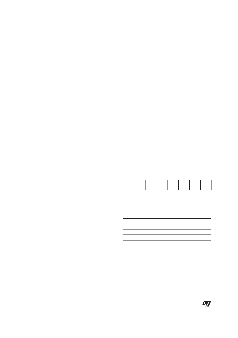
4.2.7.5 Baud Rate Register (SCBRR)
Address: 0052h
—
Read/Write
Reset Value: 00X----Xb
Contains two bits for selection of the first prescaler
factor, three bits for selection of the transmitter
rate divisor and three bits for the receiver rate divi-
sor.
excessive
Bit-7 =
SCP1
First prescaler MSB
Bit-6 =
SCP0
First prescaler LSB
These 2 prescaling bits allow several standard
clock division ranges:
Bit-5 =
SCT2
Transmitter rate divisor MSB
Bit-4 =
SCT1
Transmitter rate divisor NSB
Bit-3 =
SCT0
Transmitter rate divisor LSB
These 3 bits, in conjunction with the 2 previous bits
define the total division applied to the bus clock to
yield the transmit rate clock in conventional Baud
Rate Generator mode.
7
6
5
4
3
2
1
0
SCP1
SCP0
SCT2
SCT1
SCT0
SCR2
SCR1
SCR0
SCP1
0
0
1
1
SCP0
0
1
0
1
PR Prescaling factor
1
3
4
13
相关PDF资料 |
PDF描述 |
|---|---|
| ST730C08L3 | PHASE CONTROL THYRISTORS |
| ST730C08L3L | PHASE CONTROL THYRISTORS |
| ST730C12L0 | PHASE CONTROL THYRISTORS |
| ST730C12L0L | PHASE CONTROL THYRISTORS |
| ST730C12L1 | PHASE CONTROL THYRISTORS |
相关代理商/技术参数 |
参数描述 |
|---|---|
| ST730 | 制造商:IRF 制造商全称:International Rectifier 功能描述:PHASE CONTROL THYRISTORS Hockey Puk Version |
| ST7-30 | 制造商:SUPERWORLD 制造商全称:Superworld Electronics 功能描述:POWER TRANSFORMER |
| ST-7300 | 制造商:GC Electronics 功能描述: |
| ST730186-3 | 制造商:KEMET Corporation 功能描述: 制造商:KET 功能描述: |
| ST730268-1 | 制造商:KEMET Corporation 功能描述: 制造商:KET 功能描述: |
发布紧急采购,3分钟左右您将得到回复。