- 您现在的位置:买卖IC网 > PDF目录18758 > TRC105 (RFM)IC TXRX 300MHZ-510MHZ 32TQFN PDF资料下载
参数资料
| 型号: | TRC105 |
| 厂商: | RFM |
| 文件页数: | 15/67页 |
| 文件大小: | 0K |
| 描述: | IC TXRX 300MHZ-510MHZ 32TQFN |
| 标准包装: | 1 |
| 频率: | 300MHz ~ 510MHz |
| 数据传输率 - 最大: | 200kbps |
| 调制或协议: | FSK,OOK |
| 应用: | 通用 |
| 功率 - 输出: | 13dBm |
| 灵敏度: | -112dBm |
| 电源电压: | 2.1 V ~ 3.6 V |
| 电流 - 接收: | 3mA |
| 电流 - 传输: | 30mA |
| 数据接口: | PCB,表面贴装 |
| 天线连接器: | PCB,表面贴装 |
| 工作温度: | -40°C ~ 85°C |
| 封装/外壳: | 32-TQFN |
| 包装: | 标准包装 |
| 产品目录页面: | 583 (CN2011-ZH PDF) |
| 其它名称: | 583-1159-6 |
第1页第2页第3页第4页第5页第6页第7页第8页第9页第10页第11页第12页第13页第14页当前第15页第16页第17页第18页第19页第20页第21页第22页第23页第24页第25页第26页第27页第28页第29页第30页第31页第32页第33页第34页第35页第36页第37页第38页第39页第40页第41页第42页第43页第44页第45页第46页第47页第48页第49页第50页第51页第52页第53页第54页第55页第56页第57页第58页第59页第60页第61页第62页第63页第64页第65页第66页第67页
�� �
�
�Figure� 9�
�Note� that� start� pattern� detection� is� enabled� only� if� data� and� clock� recovery� is� enabled.�
�3.4� RSSI�
�The� received� signal� strength� is� measured� in� the� amplifier� chains� behind� the� second� mixers.� Each� amplifier� chain�
�is� composed� of� 11� amplifiers� each� having� a� gain� of� 6� dB� and� an� intermediate� output� at� 3� dB.� By� monitoring� the�
�two� outputs� of� each� stage,� an� estimation� of� the� signal� strength� with� a� resolution� of� 3� dB� and� a� dynamic� range� of�
�63� dB� is� obtained.� This� estimation� is� performed� 16� times� over� a� period� of� the� I� and� Q� signals� and� the� 16� samples�
�are� averaged� to� obtain� a� final� RSSI� value� with� a� 0.5� dB� step.� The� period� of� the� I� and� Q� signal� is� the� inverse� of� the�
�deviation� frequency,� which� is� the� low-IF� frequency� in� OOK� mode.� The� RSSI� effective� dynamic� range� can� be� in-�
�creased� to� 70� dB� by� adjusting� MCFG01_IF_Gain[1..0]� for� less� gain� on� high� signal� levels.�
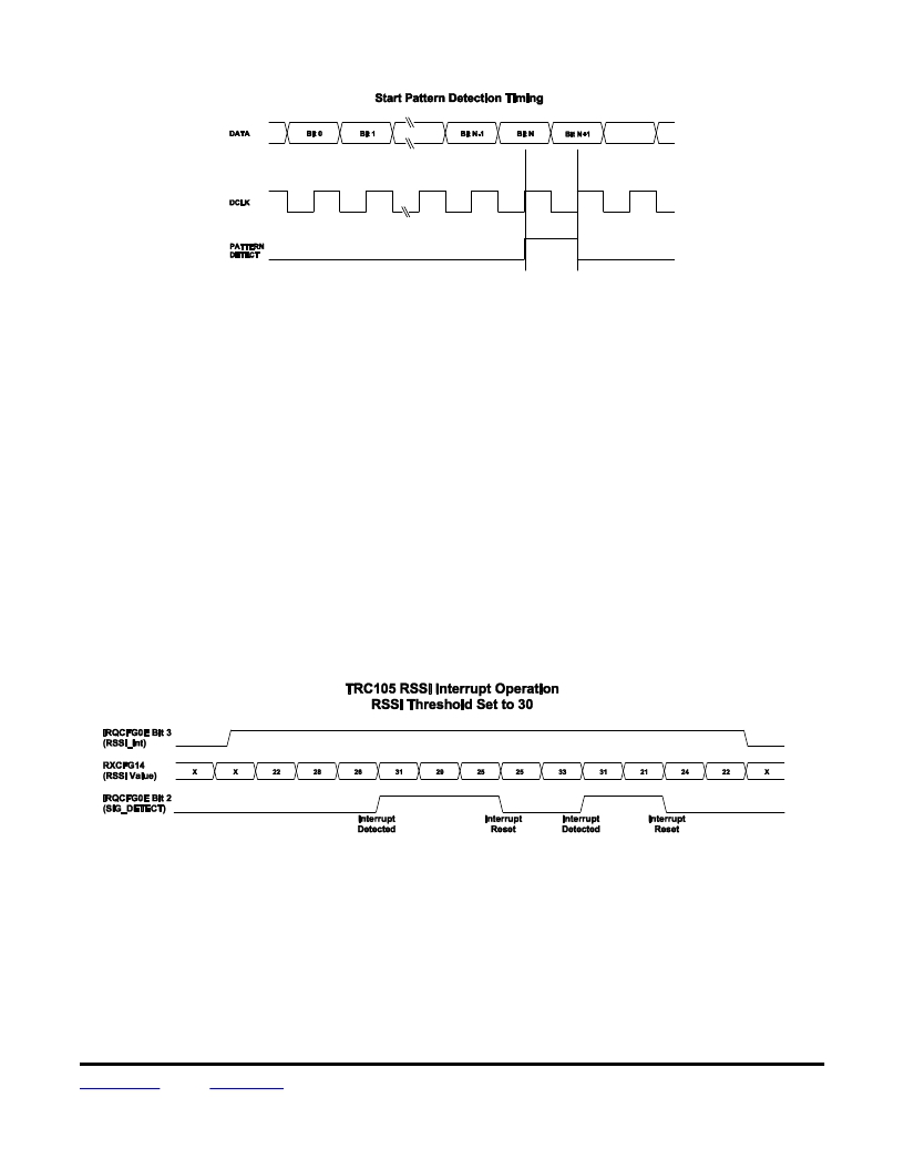
�The� RSSI� block� can� also� be� used� in� interrupt� mode� by� setting� the� bit� IRQCFG0E_RSSI_Int[3]� to� 1.� When�
�RXCFG14_RSSI� is� equal� or� greater� than� a� predefined� value� stored� in� IRQCFG0F_RSSI_thld� ,� bit� IRQCFG0E_�
�SIG_DETECT[2]� goes� high� and� an� interrupt� signal� RSSI_IRQ� is� generated� on� pin� IRQ0� if� IRQCFG0D_RX_�
�IRQ0[7..6]� is� set� to� 01� (see� Table� 10).� The� interrupt� is� cleared� by� writing� a� 1� to� bit� IRQCFG0E_� SIG_DETECT[2]� .�
�If� the� bit� RSSI_IRQ� remains� high,� the� process� starts� again.� Figure� 10� shows� the� timing� diagram� of� RSSI� in� inter-�
�rupt� mode.�
�Figure� 10�
�3.5� Receiving� in� Buffered� Data� Mode�
�The� receiver� works� in� Buffered� data� mode� when� the� MCFG01_Mode[7..6]� bits� are� set� to� 01.� In� this� mode,� the�
�output� of� the� data� and� clock� recovery,� i.e.,� the� demodulated� and� resynchronized� signal� and� the� clock� signal� DCLK�
�are� not� sent� directly� to� the� output� pins� DATA� and� IRQ1� (DCLK).� These� signals� are� used� to� store� the� demodulated�
�data� in� blocks� of� 8� bits� in� a� 64-byte� FIFO.� Figure� 11� shows� the� receiver� chain� in� this� mode.� The� FSK� and� OOK�
�demodulators,� data� and� clock� recovery� circuit� and� start� pattern� detect� block� work� as� described� for� Continuous�
�data� mode,� but� they� are� used� with� two� additional� blocks,� the� FIFO� and� SPI.�
�www.RFM.com� E-mail:� info@rfm.com�
�?� 2009-2013� by� RF� Monolithics,� Inc.�
�Technical� support� +1.800.704.6079�
�Page� 15� of� 67�
�TRC105� -� 05/29/13�
�相关PDF资料 |
PDF描述 |
|---|---|
| MT-6-15 | XFRMR 115V 5V 1.75A 6VA 3OUT |
| IF-2-10 | XFRMR 115/230V 5V 400MA 2VA PCB |
| 14A-20-515 | XFRMR PWR 115/230V 5V 750MA 20VA |
| 14A-20-512 | XFRMR PWR 115/230V 5V 750MA 20VA |
| SI4421-A0-FT | IC TXRX FSK 915MHZ 3.8V 16-TSSOP |
相关代理商/技术参数 |
参数描述 |
|---|---|
| TRC1053 | 制造商:未知厂家 制造商全称:未知厂家 功能描述:10/100M Single Port Transformer Modules |
| TRC1060 | 制造商:未知厂家 制造商全称:未知厂家 功能描述:10/100M Single Port Transformer Modules |
| TRC1062 | 制造商:未知厂家 制造商全称:未知厂家 功能描述:10/100M Single Port Transformer Modules |
| TRC1068 | 制造商:未知厂家 制造商全称:未知厂家 功能描述:10/100M Single Port Transformer Modules |
| TRC1074 | 制造商:未知厂家 制造商全称:未知厂家 功能描述:10/100M Single Port Transformer Modules |
发布紧急采购,3分钟左右您将得到回复。