- 您现在的位置:买卖IC网 > PDF目录18758 > TRC105 (RFM)IC TXRX 300MHZ-510MHZ 32TQFN PDF资料下载
参数资料
| 型号: | TRC105 |
| 厂商: | RFM |
| 文件页数: | 27/67页 |
| 文件大小: | 0K |
| 描述: | IC TXRX 300MHZ-510MHZ 32TQFN |
| 标准包装: | 1 |
| 频率: | 300MHz ~ 510MHz |
| 数据传输率 - 最大: | 200kbps |
| 调制或协议: | FSK,OOK |
| 应用: | 通用 |
| 功率 - 输出: | 13dBm |
| 灵敏度: | -112dBm |
| 电源电压: | 2.1 V ~ 3.6 V |
| 电流 - 接收: | 3mA |
| 电流 - 传输: | 30mA |
| 数据接口: | PCB,表面贴装 |
| 天线连接器: | PCB,表面贴装 |
| 工作温度: | -40°C ~ 85°C |
| 封装/外壳: | 32-TQFN |
| 包装: | 标准包装 |
| 产品目录页面: | 583 (CN2011-ZH PDF) |
| 其它名称: | 583-1159-6 |
第1页第2页第3页第4页第5页第6页第7页第8页第9页第10页第11页第12页第13页第14页第15页第16页第17页第18页第19页第20页第21页第22页第23页第24页第25页第26页当前第27页第28页第29页第30页第31页第32页第33页第34页第35页第36页第37页第38页第39页第40页第41页第42页第43页第44页第45页第46页第47页第48页第49页第50页第51页第52页第53页第54页第55页第56页第57页第58页第59页第60页第61页第62页第63页第64页第65页第66页第67页
�� �
�
�Figure� 20� shows� the� timing� diagram� for� a� single� byte� write� sequence� to� the� TRC105� through� the� SPI� configuration�
�interface.� Note� that� nSS_CONFIG� must� remain� low� during� the� transmission� of� the� two� bytes� (address� and� data).� If�
�it� goes� high� after� the� first� byte,� then� the� next� byte� will� be� considered� as� an� address� byte.� When� writing� to� more�
�than� one� register� successively,� nSS_CONFIG� does� not� need� to� have� a� high-to-low� transition� between� two� write�
�sequences.� The� bytes� are� alternatively� considered� as� an� address� byte� followed� by� a� data� byte.�
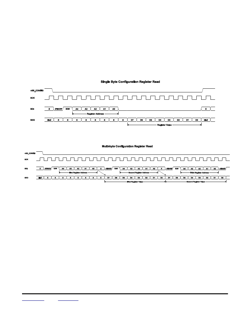
�The� read� sequence� through� the� SPI� configuration� interface� is� similar� to� the� write� sequence.� The� host� microcon-�
�troller� sends� the� address� during� the� first� SPI� communication� and� then� reads� the� data� during� a� second� SPI� com-�
�munication.� Note� that� 0� bits� can� be� input� to� the� SDI� during� the� second� SPI� communication� for� a� single� byte� read.�
�Figure� 21� shows� the� timing� diagram� for� a� single� byte� read� sequence� from� the� TRC105� through� the� SPI.�
�Figure� 21�
�Figure� 22�
�Multiple� configuration� register� reads� are� also� possible� by� sending� a� series� of� register� addresses� into� the� SPI� port,�
�as� shown� in� Figure� 22.�
�3.11� SPI� Data� FIFO� Interface�
�When� the� transceiver� is� used� in� Buffered� or� Packet� data� mode,� data� is� written� to� and� read� from� the� FIFO� through�
�the� SPI� interface.� Two� interrupts,� IRQ0� and� IRQ1,� are� used� to� manage� the� transfer� procedure.�
�When� the� transceiver� is� operating� in� Buffered� or� Packet� data� mode,� the� FIFO� interface� is� selected� when�
�nSS_DATA� is� set� to� 0� and� nSS_CONFIG� is� set� to� 1.� SPI� operations� with� the� FIFO� are� similar� to� operations� with�
�the� configuration� registers� with� two� important� exceptions.� First,� no� addresses� are� used� with� the� FIFO,� only� data�
�bytes� are� exchanged.� Second,� nSS_DATA� must� be� toggled� high� and� back� low� between� data� bytes� when� writing�
�to� the� FIFO� or� reading� from� the� FIFO.� Toggling� nSS_DATA� indexes� the� access� pointer� to� each� byte� in� the� FIFO� in�
�lieu� of� using� explicit� addressing.� Figure� 23� shows� the� timing� diagram� for� a� multiple-byte� write� sequence� to� the�
�TRC105� during� transmit,� and� Figure� 24� shows� the� timing� for� a� multi-byte� read� sequence.�
�www.RFM.com� E-mail:� info@rfm.com�
�?� 2009-2013� by� RF� Monolithics,� Inc.�
�Technical� support� +1.800.704.6079�
�Page� 27� of� 67�
�TRC105� -� 05/29/13�
�相关PDF资料 |
PDF描述 |
|---|---|
| MT-6-15 | XFRMR 115V 5V 1.75A 6VA 3OUT |
| IF-2-10 | XFRMR 115/230V 5V 400MA 2VA PCB |
| 14A-20-515 | XFRMR PWR 115/230V 5V 750MA 20VA |
| 14A-20-512 | XFRMR PWR 115/230V 5V 750MA 20VA |
| SI4421-A0-FT | IC TXRX FSK 915MHZ 3.8V 16-TSSOP |
相关代理商/技术参数 |
参数描述 |
|---|---|
| TRC1053 | 制造商:未知厂家 制造商全称:未知厂家 功能描述:10/100M Single Port Transformer Modules |
| TRC1060 | 制造商:未知厂家 制造商全称:未知厂家 功能描述:10/100M Single Port Transformer Modules |
| TRC1062 | 制造商:未知厂家 制造商全称:未知厂家 功能描述:10/100M Single Port Transformer Modules |
| TRC1068 | 制造商:未知厂家 制造商全称:未知厂家 功能描述:10/100M Single Port Transformer Modules |
| TRC1074 | 制造商:未知厂家 制造商全称:未知厂家 功能描述:10/100M Single Port Transformer Modules |
发布紧急采购,3分钟左右您将得到回复。